User:Ashmanskas/p364/2012/lab11b
From LaPET electronics
Contents |
PHYS 364, fall 2012, lab 11b
- i.e. day two of Lab #11: Monday, Nov 26
Last week, we implemented some purely combinational logic in the Xilinx FPGA, using the Verilog programming language. When we left off, we had made a 4-bit adder add up the two 4-bit numbers specified by the positions of the 8 sliding switches, and we displayed the adder's outputs on 5 green LEDs. The one piece of sequential logic that we implemented was a single SR latch, which could remember whether the set or the reset button had been pressed more recently, as indicated by lighting (or not lighting) an LED to display the latch's Q state.
- Here is a link to last week's lab: lab11.pdf
- Here is a link to last week's reading: reading11.pdf
Part 1
Let's start out today by programming the FPGA to implement the 4-bit counter that we worked through in last week's reading:
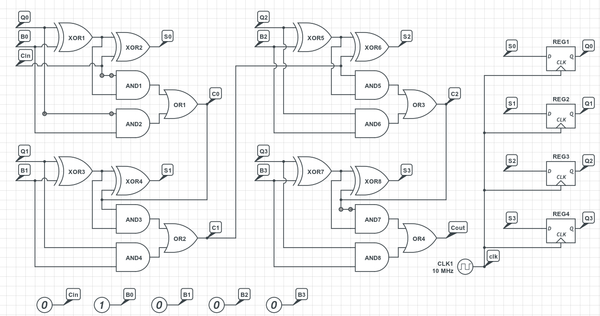
This counter consists of a 4-bit adder and four D-type flip-flops. The counter's present value is represented by the states of the four flip-flop outputs: Q3,Q2,Q1,Q0. On each clock cycle, the constant binary value 0001 is added to the counter's present value.
Here was the verilog code for the adder:
// This is the 4-bit adder circuit that we saw in
// the reading assignment.  It's the second version,
// which includes carry-in and carry-out pins, so that
// in principle you can chain two of them together to
// make an 8-bit adder, etc.
module add4bit (output cout, output s3, output s2, output s1, output s0,
		input a3, input a2, input a1, input a0,
		input b3, input b2, input b1, input b0, input cin);
   wire   c0   = (a0 & b0) | (a0 & cin) | (b0 & cin);
   wire   c1   = (a1 & b1) | (a1 & c0)  | (b1 & c0);
   wire   c2   = (a2 & b2) | (a2 & c1)  | (b2 & c1);
   assign cout = (a3 & b3) | (a3 & c2)  | (b3 & c2);
   assign s0   = a0 ^ b0 ^ cin;
   assign s1   = a1 ^ b1 ^ c0;
   assign s2   = a2 ^ b2 ^ c1;
   assign s3   = a3 ^ b3 ^ c2;
endmodule
It turns out that the following recipe is how you tell Verilog to make a D-type flip-flop. For the moment, just treat it as a magic incantation. I will put some explanation of what it means into the reading. The basic idea is that whereas a wire merely connects two things together (like a wire on your breadboard), a reg can maintain an internal state. The statement always @ (posedge clk) q_reg <= d; tells Verilog that every time it detects a positive edge (i.e. a zero-to-one transition) on the clk input, it should update q_reg to reflect the present state of the d input.
// This magic incantation is how you tell the Xilinx
// compiler to make a D-type flip-flop.  Just accept
// it as an idiom, rather than trying at this stage
// to follow exactly what the syntax means.  But the
// jist of it is that whenever a positive edge of the
// clk signal is seen, the contents of d are copied to
// the new contents of 'q_reg', which in turn is wired
// to the 'q' output of this circuit.  We will use this
// module in parts 4 and 5.
module dflipflop (output q, input clk, input d);
   reg q_reg;
   always @ (posedge clk) q_reg <= d;
   assign q = q_reg;
endmodule
Putting all of the pieces together looks like this:
//
// lab11b.v
// Verilog source code for Lab 11b
// PHYS 364, UPenn, fall 2012
//

`default_nettype none

module lab11b
  (
   input        mclk,  // 25 MHz clock built into the BASYS2 board
   output [6:0] seg,   // red 7-segment display to draw numbers & letters
   output       dp,    // decimal point for 7-seg (0=ON, 1=OFF)
   output [3:0] an,    // shared LED anode signal per 7-seg digit (0=ON)
   output [7:0] led,   // 8 green LEDs, just above sliding switches
   input  [7:0] sw,    // 8 sliding switches (up=1, down=0)
   input  [3:0] btn,   // 4 push buttons (normal=0, pushed=1)
   input  [4:1] ja,    // 4 pins (JA, NW corner) can connect to breadboard
   input  [4:1] jb,    // 4 pins (JB) can connect to breadboard
   input  [4:1] jc,    // 4 pins (JC) can connect to breadboard
   input  [4:1] jd     // 4 pins (JD, NE corner) can connect to breadboard
   );

    // an[3] is Q, btn[0] is SET, btn[1] is RESET, for SR latch
    wire srq;
    srlatch mysr1 (srq, btn[0], btn[1]);
    // make the left-most 7-segment LED light up if Q is true
    assign an[3] = ~srq;

    // We will use the 'Q' output of the SR latch as a clock
    // for the counter's flip-flops, so that we can clock the
    // counter by hand, one clock cycle at a time.
    wire clock = srq;

    // Define wires for the adder's S (sum) and COUT (carry) outputs
    wire s3, s2, s1, s0, cout;
    // The adder's CIN (carry in) will always be zero
    wire cin = 0;
    // The adder's B input will always be binary constant 0001
    wire b3=0, b2=0, b1=0, b0=1;
    // The adder's A inputs will be the flip flops' Q outputs
    wire q3, q2, q1, q0;
    add4bit myadder1 (cout,
		      s3, s2, s1, s0,
		      q3, q2, q1, q0,
		      b3, b2, b1, b0, cin);
    // Each flip-flop's D input will be one of the adder's
    // S (sum) output bits
    dflipflop mydff3 (q3, clock, s3);
    dflipflop mydff2 (q2, clock, s2);
    dflipflop mydff1 (q1, clock, s1);
    dflipflop mydff0 (q0, clock, s0);

    // Let the left four LEDs show the adder's S (sum) outputs
    assign led[7] = s3;
    assign led[6] = s2;
    assign led[5] = s1;
    assign led[4] = s0;

    // Let the right four LEDs show the flip flops' Q outputs
    assign led[3] = q3;
    assign led[2] = q2;
    assign led[1] = q1;
    assign led[0] = q0;

   // These outputs are currently unused, but I connect them anyway to
   // keep the compiler from complaining.
    assign seg[6:0] = 0;
    assign dp = 0;
    assign an[2:0] = ~btn[2:0];
endmodule


// This is the 4-bit adder circuit that we saw in
// the reading assignment.  It's the second version,
// which includes carry-in and carry-out pins, so that
// in principle you can chain two of them together to
// make an 8-bit adder, etc.
module add4bit (output cout, output s3, output s2, output s1, output s0,
		input a3, input a2, input a1, input a0,
		input b3, input b2, input b1, input b0, input cin);
   wire   c0   = (a0 & b0) | (a0 & cin) | (b0 & cin);
   wire   c1   = (a1 & b1) | (a1 & c0)  | (b1 & c0);
   wire   c2   = (a2 & b2) | (a2 & c1)  | (b2 & c1);
   assign cout = (a3 & b3) | (a3 & c2)  | (b3 & c2);
   assign s0   = a0 ^ b0 ^ cin;
   assign s1   = a1 ^ b1 ^ c0;
   assign s2   = a2 ^ b2 ^ c1;
   assign s3   = a3 ^ b3 ^ c2;
endmodule


// This magic incantation is how you tell the Xilinx
// compiler to make a D-type flip-flop.  Just accept
// it as an idiom, rather than trying at this stage
// to follow exactly what the syntax means.  But the
// jist of it is that whenever a positive edge of the
// clk signal is seen, the contents of d are copied to
// the new contents of 'q_reg', which in turn is wired
// to the 'q' output of this circuit.  We will use this
// module in parts 4 and 5.
module dflipflop (output q, input clk, input d);
    reg q_reg;
    always @ (posedge clk) q_reg <= d;
    assign q = q_reg;
endmodule


// This module implements the SR latch that we studied in Reading #11.
// You draw two NOR gates.  The output of the first NOR gate is called
// 'q'.  The output of the second NOR gate is called 'qbar' (i.e. the
// opposite of 'q').  The first NOR gate's inputs are connected to r
// (reset) and qbar.  The second NOR gate's inputs are connected to s
// (set) and q.  Normally, neither r nor s is asserted, and q keeps
// its previous state.  If you assert r (but not s), then q goes to 0.
// If you assert s (but not r), then q goes to 1.  An undefined state
// results if r and s are asserted together.
module srlatch (output q, input s, input r);
    // We define the wire 'qbar' here, but we don't connect it to
    // anything, because using it as the output argument of the second
    // nor_gate will connect it.  You can see that the wire called
    // 'qbar' connects the output of the second NOR gate to an input
    // of the first NOR gate, just as you would do if you were drawing
    // a schematic diagram of an SR latch.
    wire qbar;
    nor mynorgate1 (qbar, q, s);
    nor mynorgate2 (q, qbar, r);
endmodule
- Download lab11b.v and basys2.ucf and create and compile a new Xilinx ISE project, as you did in Part 3 of last week's lab.
- Notice that we connected one of the adder's two inputs to the binary constant 0001 and the other input to the 'Q' outputs of the four flip-flops. On each rising edge of the clock signal, the sum increments by 1.
- Notice that the 4-bit output of the adder is displayed on LEDs 7,6,5,4, and notice that the 4 flip-flop Q outputs are displayed on LEDs 3,2,1,0.
- For a clock signal, we are using the Q output of an SR latch, whose reset input is button 1 and whose set input is button 0. You can monitor the present value of the latch's Q output by looking at the left-most digit of the 7-segment display. By alternately pressing buttons 1 and 0, you can manually clock the counter.
- Try clocking the counter by pushing (alternately) buttons 1 and 0.
- Notice that the four Q bits are always one clock cycle behind the four S bits. In other words, the value displayed on the right 4 LEDs just after the clock edge is the value that had been displayed on the left 4 LEDs just before the clock edge.
- Take the time to understand how the Verilog code is equivalent to the schematic diagram shown above.
- Now modify the program so that the B input bits to the adder are the switch values sw[3], sw[2], sw[1], sw[0] instead of the constant values 0, 0, 0, 1.
- Now you will need to set the right four switches to DOWN, DOWN, DOWN, UP to get the counter to count up by ones. Give it a try.
- Can you make the counter count up by twos? By threes?
- What settings should you use on the four switches to make your counter count DOWN by ones? Hint: do you remember the 4-bit two's complement representation for -1 ?
Part 2
Now we're going to connect 8 D-type flipflops together into a shift register. This configuration is also known as a pipeline, because data flows from one flip-flop to the next on each clock cycle, as if it were moving through a pipe.
The schematic diagram looks something like this, though I only drew 4 of the 8 flip-flops here:
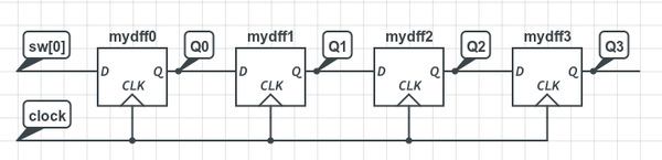
Here is the Verilog code that is equivalent to the above schematic (but with 8 DFFs instead of just 4):
    // The first flip-flop's D input will be sw[0] (the right-most
    // switch).  Each subsequent flip-flop's D input will be the
    // previous flip-flop's Q output.
    wire q7, q6, q5, q4, q3, q2, q1, q0;
    dflipflop mydff0 (q0, clock, sw[0]);
    dflipflop mydff1 (q1, clock, q0);
    dflipflop mydff2 (q2, clock, q1);
    dflipflop mydff3 (q3, clock, q2);
    dflipflop mydff4 (q4, clock, q3);
    dflipflop mydff5 (q5, clock, q4);
    dflipflop mydff6 (q6, clock, q5);
    dflipflop mydff7 (q7, clock, q6);
Notice that each flip-flop's D input is connected to the previous flip-flop's Q output.
We also send all of the Q outputs to the 8 green LEDs:
    // Display the 8 flip flops' Q values on the 8 green LEDs.
    assign led[7] = q7;
    assign led[6] = q6;
    assign led[5] = q5;
    assign led[4] = q4;
    assign led[3] = q3;
    assign led[2] = q2;
    assign led[1] = q1;
    assign led[0] = q0;
Here is the complete program, which you can copy and paste into the Xilinx editor in place of the version of lab11b.v that you have there now:
//
// lab11b.v
// Verilog source code for Lab 11b (part 2)
// PHYS 364, UPenn, fall 2012
//

`default_nettype none

module lab11b
  (
   input        mclk,  // 25 MHz clock built into the BASYS2 board
   output [6:0] seg,   // red 7-segment display to draw numbers & letters
   output       dp,    // decimal point for 7-seg (0=ON, 1=OFF)
   output [3:0] an,    // shared LED anode signal per 7-seg digit (0=ON)
   output [7:0] led,   // 8 green LEDs, just above sliding switches
   input  [7:0] sw,    // 8 sliding switches (up=1, down=0)
   input  [3:0] btn,   // 4 push buttons (normal=0, pushed=1)
   input  [4:1] ja,    // 4 pins (JA, NW corner) can connect to breadboard
   input  [4:1] jb,    // 4 pins (JB) can connect to breadboard
   input  [4:1] jc,    // 4 pins (JC) can connect to breadboard
   input  [4:1] jd     // 4 pins (JD, NE corner) can connect to breadboard
   );

    // an[3] is Q, btn[0] is SET, btn[1] is RESET, for SR latch
    wire srq;
    srlatch mysr1 (srq, btn[0], btn[1]);
    // make the left-most 7-segment LED light up if Q is true
    assign an[3] = ~srq;

    // We will use the 'Q' output of the SR latch as a clock
    // for the counter's flip-flops, so that we can clock the
    // counter by hand, one clock cycle at a time.
    wire clock = srq;

    // The first flip-flop's D input will be sw[0] (the right-most
    // switch).  Each subsequent flip-flop's D input will be the
    // previous flip-flop's Q output.
    wire q7, q6, q5, q4, q3, q2, q1, q0;
    dflipflop mydff0 (q0, clock, sw[0]);
    dflipflop mydff1 (q1, clock, q0);
    dflipflop mydff2 (q2, clock, q1);
    dflipflop mydff3 (q3, clock, q2);
    dflipflop mydff4 (q4, clock, q3);
    dflipflop mydff5 (q5, clock, q4);
    dflipflop mydff6 (q6, clock, q5);
    dflipflop mydff7 (q7, clock, q6);

    // Display the 8 flip flops' Q values on the 8 green LEDs.
    assign led[7] = q7;
    assign led[6] = q6;
    assign led[5] = q5;
    assign led[4] = q4;
    assign led[3] = q3;
    assign led[2] = q2;
    assign led[1] = q1;
    assign led[0] = q0;

   // These outputs are currently unused, but I connect them anyway to
   // keep the compiler from complaining.
    assign seg[6:0] = 0;
    assign dp = 0;
    assign an[2:0] = ~btn[2:0];
endmodule


// This magic incantation is how you tell the Xilinx
// compiler to make a D-type flip-flop.  Just accept
// it as an idiom, rather than trying at this stage
// to follow exactly what the syntax means.  But the
// jist of it is that whenever a positive edge of the
// clk signal is seen, the contents of d are copied to
// the new contents of 'q_reg', which in turn is wired
// to the 'q' output of this circuit.  We will use this
// module in parts 4 and 5.
module dflipflop (output q, input clk, input d);
    reg q_reg;
    always @ (posedge clk) q_reg <= d;
    assign q = q_reg;
endmodule


// This module implements the SR latch that we studied in Reading #11.
// You draw two NOR gates.  The output of the first NOR gate is called
// 'q'.  The output of the second NOR gate is called 'qbar' (i.e. the
// opposite of 'q').  The first NOR gate's inputs are connected to r
// (reset) and qbar.  The second NOR gate's inputs are connected to s
// (set) and q.  Normally, neither r nor s is asserted, and q keeps
// its previous state.  If you assert r (but not s), then q goes to 0.
// If you assert s (but not r), then q goes to 1.  An undefined state
// results if r and s are asserted together.
module srlatch (output q, input s, input r);
    // We define the wire 'qbar' here, but we don't connect it to
    // anything, because using it as the output argument of the second
    // nor_gate will connect it.  You can see that the wire called
    // 'qbar' connects the output of the second NOR gate to an input
    // of the first NOR gate, just as you would do if you were drawing
    // a schematic diagram of an SR latch.
    wire qbar;
    nor mynorgate1 (qbar, q, s);
    nor mynorgate2 (q, qbar, r);
endmodule
- Once you have the program compiled and loaded into your FPGA board, try clocking the flip-flops by alternately pressing buttons 1 and 0. If you do this with SW0 in the DOWN position, you should see nothing very interesting happen.
- Now set SW0 to the UP position. You should see the LEDs light up one-by-one.
- Try setting SW0 back to the DOWN position, You should see darkness shift left clock-by-clock in the same as as you saw light shifting left before.
- Keep clocking in ZEROs until all of the LEDs are off. Now clock in a single ONE bit. In other words, flip SW0 to UP, then do a single clock cycle, then flip SW0 back to DOWN, then keep clocking. Do you see how the single ONE bit shifts from right to left?
- A shift-register is sometimes used to delay data so that they can be kept around while a lengthy computation completes. The length of a shift register is analogous to the length of the pipeline on your home computer's microprocessor.
Part 3
- Now here is a slightly different kind of D-type flip-flop. It has an additional input called ENABLE.
// This magic incantation is how you tell the Xilinx compiler to make
// a D-type flip-flop with the ENABLE feature.
module dffe (output q, input clk, input d, input enable);
    reg q_reg;
    always @ (posedge clk) if (enable) q_reg <= d;
    assign q = q_reg;
endmodule
We're going to modify the main part of the part 2 program to look like this instead:
    // Now we set up 8 D-type flip-flops that have an additional
    // input wire called ENABLE.  If ENABLE is TRUE, then the
    // flip-flop behaves exactly as an ordinary DFF.  But if ENABLE
    // is FALSE, then the DFF does nothing.

    // Now we connect each flip flop's D input to the NOT of its own
    // Q output.  So if ENABLE is asserted, the flip-flop just toggles
    // back and forth between 0 and 1.  But if ENABLE is deasserted,
    // the flip-flop does nothing.
    wire q7, q6, q5, q4, q3, q2, q1, q0;
    wire d7 = ~q7;
    wire d6 = ~q6;
    wire d5 = ~q5;
    wire d4 = ~q4;
    wire d3 = ~q3;
    wire d2 = ~q2;
    wire d1 = ~q1;
    wire d0 = ~q0;

    // Here is the tricky part:  the first flip flop is always enabled.
    // The second flip flop is only enabled if the first one is HIGH.
    // The third flip flop is only enabled if the first two are HIGH.
    // The fourth is only enabled if the first three are HIGH.  Etc.
    wire e0 = 1;
    wire e1 = q0;
    wire e2 = q0 & q1;
    wire e3 = q0 & q1 & q2;
    wire e4 = q0 & q1 & q2 & q3;
    wire e5 = q0 & q1 & q2 & q3 & q4;
    wire e6 = q0 & q1 & q2 & q3 & q4 & q5;
    wire e7 = q0 & q1 & q2 & q3 & q4 & q5 & q6;
    dffe mydff0 (q0, clock, d0, e0);
    dffe mydff1 (q1, clock, d1, e1);
    dffe mydff2 (q2, clock, d2, e2);
    dffe mydff3 (q3, clock, d3, e3);
    dffe mydff4 (q4, clock, d4, e4);
    dffe mydff5 (q5, clock, d5, e5);
    dffe mydff6 (q6, clock, d6, e6);
    dffe mydff7 (q7, clock, d7, e7);
- Can you guess what this program will do?! See if you can figure out what it is doing and why it works.
- Here, below, I paste in the complete source code, which you can compile and load into your board.
//
// lab11b.v
// Verilog source code for Lab 11b (part 3)
// PHYS 364, UPenn, fall 2012
//

`default_nettype none

module lab11b
  (
   input        mclk,  // 25 MHz clock built into the BASYS2 board
   output [6:0] seg,   // red 7-segment display to draw numbers & letters
   output       dp,    // decimal point for 7-seg (0=ON, 1=OFF)
   output [3:0] an,    // shared LED anode signal per 7-seg digit (0=ON)
   output [7:0] led,   // 8 green LEDs, just above sliding switches
   input  [7:0] sw,    // 8 sliding switches (up=1, down=0)
   input  [3:0] btn,   // 4 push buttons (normal=0, pushed=1)
   input  [4:1] ja,    // 4 pins (JA, NW corner) can connect to breadboard
   input  [4:1] jb,    // 4 pins (JB) can connect to breadboard
   input  [4:1] jc,    // 4 pins (JC) can connect to breadboard
   input  [4:1] jd     // 4 pins (JD, NE corner) can connect to breadboard
   );

    // an[3] is Q, btn[0] is SET, btn[1] is RESET, for SR latch
    wire srq;
    srlatch mysr1 (srq, btn[0], btn[1]);
    // make the left-most 7-segment LED light up if Q is true
    assign an[3] = ~srq;

    // We will use the 'Q' output of the SR latch as a clock
    // for the counter's flip-flops, so that we can clock the
    // counter by hand, one clock cycle at a time.
    wire clock = srq;

    // Now we set up 8 D-type flip-flops that have an additional
    // input wire called ENABLE.  If ENABLE is TRUE, then the
    // flip-flop behaves exactly as an ordinary DFF.  But if ENABLE
    // is FALSE, then the DFF does nothing.

    // Now we connect each flip flop's D input to the NOT of its own
    // Q output.  So if ENABLE is asserted, the flip-flop just toggles
    // back and forth between 0 and 1.  But if ENABLE is deasserted,
    // the flip-flop does nothing.
    wire q7, q6, q5, q4, q3, q2, q1, q0;
    wire d7 = ~q7;
    wire d6 = ~q6;
    wire d5 = ~q5;
    wire d4 = ~q4;
    wire d3 = ~q3;
    wire d2 = ~q2;
    wire d1 = ~q1;
    wire d0 = ~q0;

    // Here is the tricky part:  the first flip flop is always enabled.
    // The second flip flop is only enabled if the first one is HIGH.
    // The third flip flop is only enabled if the first two are HIGH.
    // The fourth is only enabled if the first three are HIGH.  Etc.
    wire e0 = 1;
    wire e1 = q0;
    wire e2 = q0 & q1;
    wire e3 = q0 & q1 & q2;
    wire e4 = q0 & q1 & q2 & q3;
    wire e5 = q0 & q1 & q2 & q3 & q4;
    wire e6 = q0 & q1 & q2 & q3 & q4 & q5;
    wire e7 = q0 & q1 & q2 & q3 & q4 & q5 & q6;
    dffe mydff0 (q0, clock, d0, e0);
    dffe mydff1 (q1, clock, d1, e1);
    dffe mydff2 (q2, clock, d2, e2);
    dffe mydff3 (q3, clock, d3, e3);
    dffe mydff4 (q4, clock, d4, e4);
    dffe mydff5 (q5, clock, d5, e5);
    dffe mydff6 (q6, clock, d6, e6);
    dffe mydff7 (q7, clock, d7, e7);

    // Display the 8 flip flops' Q values on the 8 green LEDs.
    assign led[7] = q7;
    assign led[6] = q6;
    assign led[5] = q5;
    assign led[4] = q4;
    assign led[3] = q3;
    assign led[2] = q2;
    assign led[1] = q1;
    assign led[0] = q0;

   // These outputs are currently unused, but I connect them anyway to
   // keep the compiler from complaining.
    assign seg[6:0] = 0;
    assign dp = 0;
    assign an[2:0] = ~btn[2:0];
endmodule


// This magic incantation is how you tell the Xilinx compiler to make
// a D-type flip-flop with the ENABLE feature.
module dffe (output q, input clk, input d, input enable);
    reg q_reg;
    always @ (posedge clk) if (enable) q_reg <= d;
    assign q = q_reg;
endmodule


// This module implements the SR latch that we studied in Reading #11.
// You draw two NOR gates.  The output of the first NOR gate is called
// 'q'.  The output of the second NOR gate is called 'qbar' (i.e. the
// opposite of 'q').  The first NOR gate's inputs are connected to r
// (reset) and qbar.  The second NOR gate's inputs are connected to s
// (set) and q.  Normally, neither r nor s is asserted, and q keeps
// its previous state.  If you assert r (but not s), then q goes to 0.
// If you assert s (but not r), then q goes to 1.  An undefined state
// results if r and s are asserted together.
module srlatch (output q, input s, input r);
    // We define the wire 'qbar' here, but we don't connect it to
    // anything, because using it as the output argument of the second
    // nor_gate will connect it.  You can see that the wire called
    // 'qbar' connects the output of the second NOR gate to an input
    // of the first NOR gate, just as you would do if you were drawing
    // a schematic diagram of an SR latch.
    wire qbar;
    nor mynorgate1 (qbar, q, s);
    nor mynorgate2 (q, qbar, r);
endmodule
