User:Ashmanskas/p364/lecture 10
From LaPET electronics
Contents |
Lecture 10: 2010-11-15 (programmable logic, memories, state machines)
- Topics:
- Verilog notes
- Memories: ROM, SRAM, DRAM, etc.
- Finite State Machines
- Introduce microprocessor concept to be discussed next week
Verilog notes
- Let's go through the Verilog Notes I wrote up to help you to get started
Multiplexers → Memories
Consider this multiplexer from the Verilog Notes:

module mux2to1 (
    input  wire select,
    input  wire IN0,
    input  wire IN1,
    output wire OUT
);
    assign OUT = (IN0 & ~select) | (IN1 & select);
endmodule
Let's increase the number of choices from two to 256. This requires 8 select lines: 28 = 256. I draw the symbol two different ways: one using eight separate select lines, and another using an 8-bit-wide "bus" (or "vector" in Verilog) of select lines. Usually the latter is easier to read.
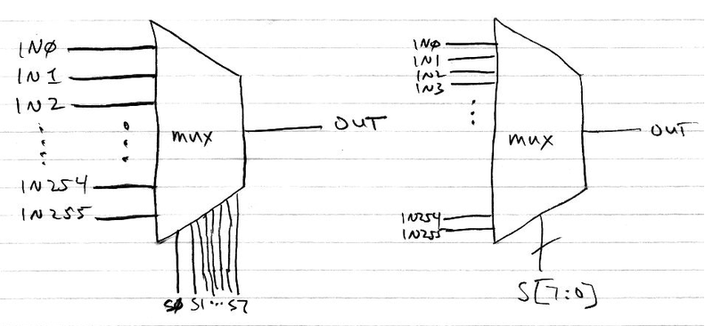
module mux256to1 (
    input  wire [7:0] S,
    input  wire IN0, IN1, IN2, IN3, IN4, IN5, IN6, IN7, IN8, IN9,
    input  wire IN10, IN11, IN12, IN13, IN14, IN15, IN16, IN17, IN18, IN19, IN20,
    ...
    input  wire IN250, IN251, IN252, IN253, IN254, IN255,
    output wire OUT
);
    assign OUT =
        (!S[7] & !S[6] & !S[5] & !S[4] & !S[3] & !S[2] & !S[1] & !S[0] & IN0)   |
        (!S[7] & !S[6] & !S[5] & !S[4] & !S[3] & !S[2] & !S[1] &  S[0] & IN1)   |
        (!S[7] & !S[6] & !S[5] & !S[4] & !S[3] & !S[2] &  S[1] & !S[0] & IN2)   |
        (!S[7] & !S[6] & !S[5] & !S[4] & !S[3] & !S[2] &  S[1] &  S[0] & IN3)   |
        ....
        ( S[7] &  S[6] &  S[5] &  S[4] &  S[3] &  S[2] &  S[1] & !S[0] & IN254) |
        ( S[7] &  S[6] &  S[5] &  S[4] &  S[3] &  S[2] &  S[1] &  S[0] & IN255) ;
endmodule
Notice that mux256to1 is just a big pile of AND gates, OR gates, and inverters. (Something like 128 inverters, 256 nine-input AND gates, and one 256-input OR gate --- so you could build it with fewer than a thousand 74HC00 chips.) Notice also that simply by connecting all of the IN0 ... IN255 to a suitable combination of 1 and 0 values, mux256to1 can implement an arbitrary 8-to-1 truth table. It can map any pattern of 8 input bits into one output bit.
An arbitrary truth table is sometimes called a lookup table. It turns out that a 4-to-1 lookup table (usually paired with a D-type flip-flop) is the basic unit of a Xilinx FPGA. http://en.wikipedia.org/wiki/Field-programmable_gate_array
Now let's repeat mux256to1 sixteen times, so that each of the 256 input choices is not a single bit but a 16-bit number.
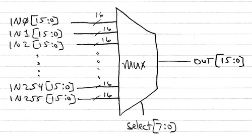
module mux256to1_16bit (
    input  wire  [7:0] S,
    input  wire [15:0] IN0, IN1, IN2, IN3, IN4, IN5, IN6, IN7, IN8, IN9,
    input  wire [15:0] IN10, IN11, IN12, IN13, IN14, IN15, IN16, IN17, IN18, IN19, IN20,
    ...
    input  wire [15:0] IN250, IN251, IN252, IN253, IN254, IN255,
    output wire [15:0] OUT
);
    mux256to1(S, IN0[0], IN1[0], IN2[0], ...., IN254[0], IN255[0], OUT[0]);
    mux256to1(S, IN0[1], IN1[1], IN2[1], ...., IN254[1], IN255[1], OUT[1]);
    mux256to1(S, IN0[2], IN1[2], IN2[2], ...., IN254[2], IN255[2], OUT[2]);
    ....
    mux256to1(S, IN0[14], IN1[14], IN2[14], ...., IN254[14], IN255[14], OUT[14]);
    mux256to1(S, IN0[15], IN1[15], IN2[15], ...., IN254[15], IN255[15], OUT[15]);
endmodule
Now we have a device that can map an arbitrary 8-bit number into an arbitrary 16-bit number, simply by arranging for all 4096 of the IN wires to be connected to the desired pattern of 1 and 0 values. Such a device is known as a Read-Only Memory, or a ROM. In this case, it would be called a 256x16 ROM.
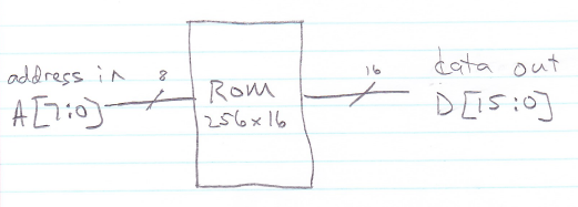
A ROM is the simplest example of a memory. A memory can store useful information. For instance, this ROM might store 16 bits of longitude and 16 bits of latitude for each of 128 cities you would like to visit on future vacations. (16 bits per geographic coordinate gives you about 0.6 kilometer precision.) Memories come in many shapes and sizes, though the number of data bits is most commonly 8, 16, or 32, and the number of storage locations is always a power of two --- it's 2n , where n is the number of address bits. In a memory, the OUT[15:0] lines would really be called data lines D[15:0] (or in some cases Q[15:0]), and the S[7:0] "select" lines would really be called address lines A[7:0].
Memories
Memory is far more useful if your circuit can write to it as well as read from it.
A memory with which you can both read and write is normally called a RAM (random access memory), though technically the "random" in RAM refers not to read/write capability but rather to the fact that you can access the addresses in any order you like. A magnetic tape drive, by contrast, allows only sequential access. There is more discussion of what the "random" really means in this context at http://en.wikipedia.org/wiki/Random-access_memory . By the wikipedia's definition, a ROM is a special case of a random access memory, since you can access the contents in any order. While this may be strictly true, nobody who is trying to communicate clearly would ever refer to read-only memory as a RAM.
For our purposes, a RAM is a memory that can be both read and written quickly at arbitrary addresses in arbitrary order. The fastest and easiest-to-use RAM is called static RAM, or SRAM. An SRAM uses one flip-flop to store each bit. (Often the flip-flop in an SRAM is formed using two inverters instead of two NAND gates, to use fewer transistors, but conceptually each memory cell is a flip-flop.) So a 256x16 SRAM would use 4096 flip-flops. Here is a straightforward implementation of a 256x1 SRAM (i.e. 256 locations, each storing 1-bit-wide data).

module sram256x1 (
    input  wire       clk,
    input  wire       wen,
    input  wire       D,
    input  wire [7:0] A,
    output wire       Q
);
    // Use address lines to demultiplex write-enable to 256 flip-flop enables
    wire wen0 = wen && A=='b00000000;
    wire wen1 = wen && A=='b00000001;
    wire wen2 = wen && A=='b00000010;
    ....
    wire wen254 = wen && A=='b11111110;
    wire wen255 = wen && A=='b11111111;
    // 256 D-type flip-flops store 1 bit for each of 256 locations
    dffe ff0 (.clk(clk), .ena(wen0), .d(D), .q(Q0));
    dffe ff1 (.clk(clk), .ena(wen1), .d(D), .q(Q1));
    ....
    dffe ff255 (.clk(clk), .ena(wen255), .d(D), .q(Q255));
    // Use address lines to multiplex 256 flip-flop outputs to data output Q
    mux256to1 mux (.S(A), .IN0(Q0), .IN1(Q1), .IN2(Q2), ...., .IN255(Q255), .OUT(Q));
endmodule
Now we can put 16 of these sram256x1 devices together to form a 256x16 SRAM, i.e. storing a 16-bit-wide value at each of 256 locations.
module sram256x16 (
    input  wire        clk,
    input  wire        wen,
    input  wire [15:0] Din,
    input  wire  [7:0] addr,
    output wire [15:0] Dout
);
    sram256x1 ram0 (.clk(clk), .wen(wen), .D(Din[0]), .A(addr), .Q(Dout[0]);
    sram256x1 ram0 (.clk(clk), .wen(wen), .D(Din[1]), .A(addr), .Q(Dout[1]);
    sram256x1 ram0 (.clk(clk), .wen(wen), .D(Din[2]), .A(addr), .Q(Dout[2]);
    ....
    sram256x1 ram14 (.clk(clk), .wen(wen), .D(Din[14]), .A(addr), .Q(Dout[14]);
    sram256x1 ram15 (.clk(clk), .wen(wen), .D(Din[15]), .A(addr), .Q(Dout[15]);
endmodule

In real life, a single data bus is normally used for both reads and writes. Having separate read and write paths would waste pins. But separate Din and Dout (or sometimes D and Q) buses are easier to use and to understand. So inside an FPGA, where there are no physical pins to worry about, one frequently uses separate buses for reading and writing a memory.
The RAM inside your computer --- nowadays measured in hundreds of megabytes, if not gigabytes --- is not SRAM. It is synchronous DRAM (SDRAM). DRAM (dynamic RAM) uses a capacitor instead of a flip-flop to hold the state of each stored bit. Since the capacitors' charge slowly leaks away, the contents of DRAM must be refreshed several times per second. In exchange for the hassle of refreshing, DRAM offers a large cost savings over SRAM: SRAM requires typically six transistors per memory cell, while DRAM requires one transistor and one capacitor per cell.
Finite State Machines
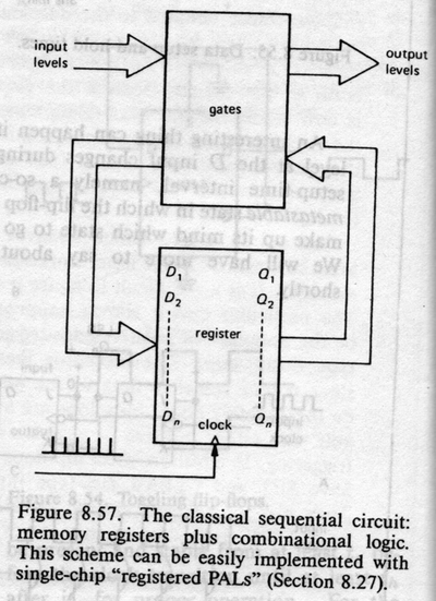
The figure above (HH figure 8.57) shows a generic sequential circuit. A Finite State Machine (FSM) is a special case of sequential circuit in which one register is designated the state number. The FSM moves from state to state when specified conditions are met. The next state is a (deterministic) function of the present state and the machine's input. The output is a function of the present state.
FSMs are ubiquitous --- and quite handy. The two most common applications that come to mind are validating ("parsing") input --- e.g. for a vending machine --- and sequencing operations --- e.g. for a traffic signal. A state machine allows you to do with a few D-type flip-flops and some combinational logic the sorts of things you may be accustomed to doing with a simple computer program. This can be helpful if the circuit you are building needs to carry out a sequence of steps to do its job.
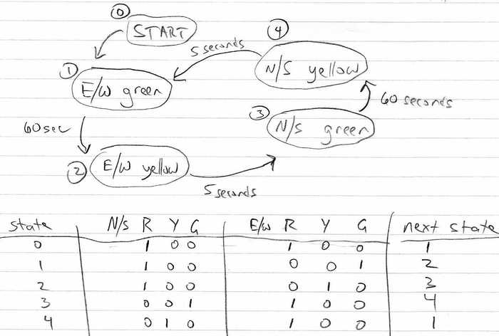
A state diagram can be very helpful for describing an FSM's intended behavior. Here is a simple traffic signal FSM:
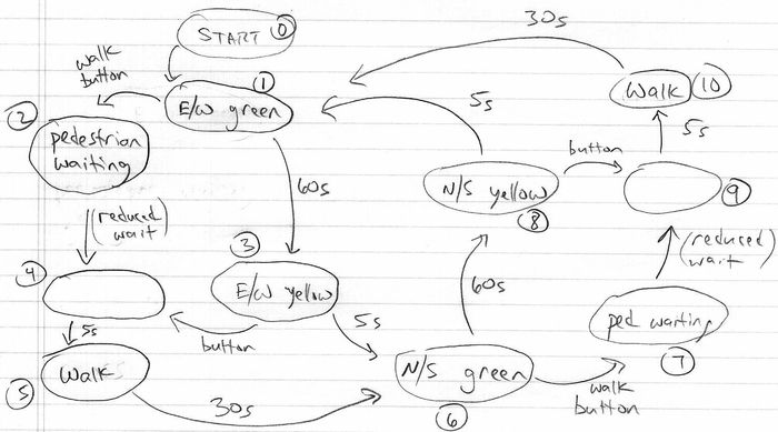
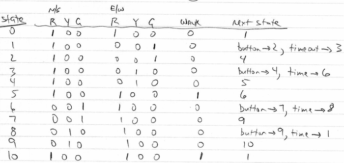
Now suppose we add a button for pedestrians to signal that they want to cross the street.
I will make a skeletal Verilog implementation of the first traffic signal FSM above --- the simpler one. Part of this week's lab will be for you to flesh out the missing details. If you're really ambitious, you can try the version with the crosswalk!
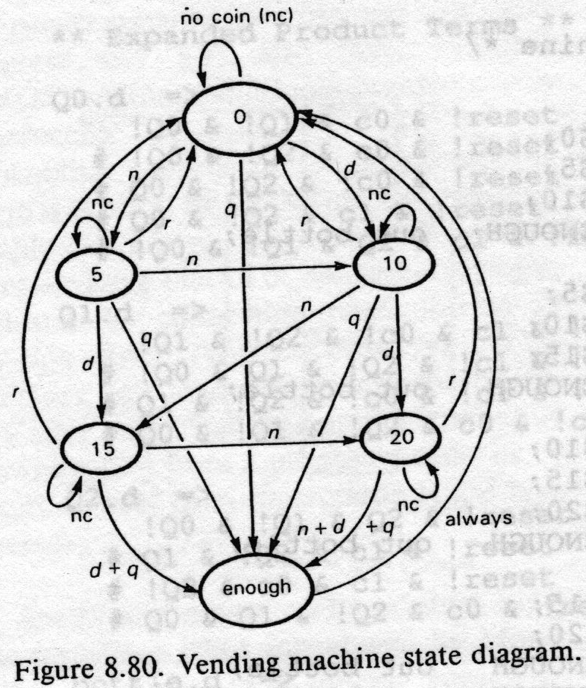
Below is a diagram from HH (figure 8.80) of a state machine for a vending machine. Let's work through an implementation of this FSM. By the way, how would you modify this machine to give back change if you overpay? What about handling canceled transactions?
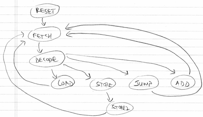
Microprocessor concept
- execute a sequence of instructions
- instructions have useful consequences, such as moving data around, performing math operations, performing input/output to the external world, etc.
- instructions are stored in memory
- program counter is the memory address of the next instruction to be executed
- program counter is one of several registers used by the microprocessor
- instruction register holds instruction currently being executed
- general-purpose registers might hold temporary results of computations
- sometimes there is an accumulator register that plays a special role in math operations
- processor has access to read/write memory for data storage
- in Von Neumann architecture (most common), program and data are stored in same memory
- you occasionally see "Harvard architecture," in which program memory and data memory are totally separate
- you write your program in C, C++, Pascal, Fortran, etc.
- compiler translates your program into low-level instructions for the microprocessor to execute
- microprocessor starts at the first address of your program, fetches instruction, decodes instruction, executes instruction, goes on to next instruction
- simple microprocessor we will discuss next week has this very minimal set of instructions: LOAD, STORE, JUMP, JUMPZ, JUMPN, ADD, SUB, MUL
- a microprocessor is basically a sophisticated Finite State Machine with an attached memory and some means of exchanging data with the outside world