User:Ashmanskas/p364/lecture 9
From LaPET electronics
Contents |
Lecture 9: 2010-11-08 (programmable logic)
A few notes
- Only Monday's lab is required this week. Feel free to skip Thursday's session, whether or not you are taking the GRE this weekend.
- If you do come to lab on Thursday, Jose and I will be there to discuss final project ideas with you.
- If you like, you can download a free copy of the Xilinx ISE "webpack" software from http://www.xilinx.com/tools/webpack.htm .
- Documentation for the Digilent CMOD board can be found at http://www.digilentinc.com/Products/Detail.cfm?Prod=CMOD
- I've written some Verilog Notes to help you to get started
Lecture
FPGA overview
This week we introduce programmable logic. After spending last week tediously connecting wires between discrete logic components, you will quickly appreciate the usefulness of Field Programmable Gate Arrays. (Technically, the Xilinx device that we will use for the next few labs -- the XC2C64A, mounted on a CMOD board from Digilent -- is a CPLD, not an FPGA. As far as I can tell, a CPLD is just a smaller and less versatile FPGA.)
The FPGA market is currently dominated by two major vendors, Altera and Xilinx. I spent about ten years (roughly 1998--2008) working with Altera FPGAs, and since 2008 I have worked with Xilinx FPGAs. From my point of view, the most substantial difference between the two vendors is the software that you use to compile your design files into bits that can be loaded into the vendors' chips. The two vendors' FPGAs offer a similar range of features. The main reason we are using a Xilinx device in this course is that Digilent sells for $18 a small Xilinx FPGA (or CPLD) mounted on a tiny circuit board that can be readily plugged into the breadboards that you already use in lab. This makes it easy for you to compare the FPGA with the discrete 74LSnn chips that you used in last week's lab.
A high-end modern FPGA contains in a single chip the equivalent of O(1 million) of the discrete logic gates that you used in Lab 8. And that chip can be reprogrammed many times to perform different functions, just by changing the program that you compile into the chip. Thus, a digital design that used to require connecting many 74LSnn components together with copper traces on a printed circuit board now just requires a sort of programming that causes logic to be internally connected within the FPGA. As a result, sophisticated digital designs are far easier to implement and enormously easier to modify in situ. (Hence "field programmable.")
There are three prevailing ways of developing FPGA programs: drawing schematic diagrams that allow you to pretend you are wiring together 74-series logic components; writing VHDL code; and writing Verilog code. I have tried all three and have a strong preference for Verilog, so that is what we will use.
Verilog was originally developed for simulating and testing logic, rather than for implementing logic, so the Verilog language contains some features that cannot be synthesized by the Xilinx compiler. (For example, a Verilog simulator can print out the value of a variable every time it changes -- something a real chip can't do on its own.) We will discuss only the synthesizable subset of Verilog (with a few exceptions, such as printing out variable contents). Nowadays I imagine that Verilog is used more often for FPGA synthesis than for generic logic simulation.
Probably the best way to start learning Verilog is just to dive in. When you have questions, you can ask me or you can consult the Verilog book chapters I handed out last week. I will start by implementing in Verilog the logic that you implemented last week with individual 74LSxx chips. In tonight's lab, you will compile these examples into your own FPGA and try them out. There may also be a couple of examples in which I give you a Verilog program that is nearly complete and you add a few lines to flesh out the details.
Then, once you've had this week to get comfortable with the FPGA and the Xilinx software, we'll make next week's lab a bit more challenging.
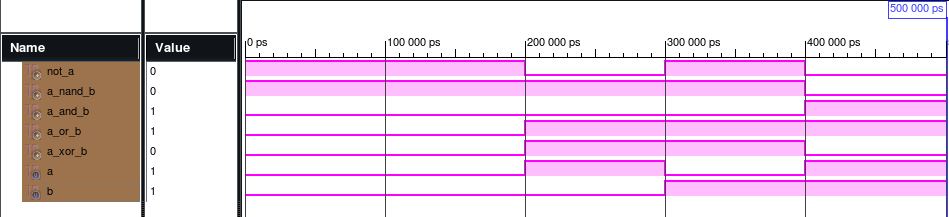
Simple gate example (NOT, NAND, AND, OR, XOR)
// nand_etc.v

`timescale 1ns / 1ps
`default_nettype none

module nand_etc
(
    input  wire a,
    input  wire b,
    output wire not_a,
    output wire a_nand_b,
    output wire a_and_b,
    output wire a_or_b,
    output wire a_xor_b
);
    assign not_a    = ~a;
    assign a_nand_b = ~(a&b);
    assign a_and_b  = a&b;
    assign a_or_b   = a|b;
    assign a_xor_b  = a^b;
endmodule
Normally you write a "test bench" for your design, so that you can try it out in the simulator before you try it on real hardware. This test bench runs inside the Xilinx "ISIM" simulator. Note that you will see the test benches use some non-synthesizable features of Verilog: explicit time delays, initial values, $finish, etc.
// nand_etc_tb.v

`timescale 1ns / 1ps
`default_nettype none

module nand_etc_tb;
    // Inputs for UUT
    reg a=0;
    reg b=0;
    // Outputs of UUT
    wire not_a;
    wire a_nand_b;
    wire a_and_b;
    wire a_or_b;
    wire a_xor_b;

    // Instantiate the Unit Under Test (UUT)
    nand_etc uut
    (
	.a(a),
	.b(b),
	.not_a(not_a),
	.a_nand_b(a_nand_b),
	.a_and_b(a_and_b),
	.a_or_b(a_or_b),
	.a_xor_b(a_xor_b)
    );

initial begin
    // Wait 100 ns for simulator reset to finish
    #100;

    // Drive first set of inputs
    a = 0; b = 0;

    // Wait 100ns then drive next set of inputs
    #100; a = 1; b = 0;

    // Wait 100ns then drive next set of inputs
    #100; a = 0; b = 1;

    // Wait 100ns then drive last set of inputs
    #100; a = 1; b = 1;

    // Wait 100ns then terminate simulation
    #100;
    $finish;
end

endmodule
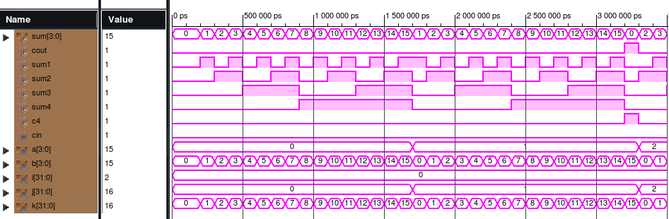
Four-bit full adder example
This first version will implement the adder using individual gates.
// fourbit_fulladder_v1.v

`timescale 1ns / 1ps
`default_nettype none

module fourbit_fulladder_v1
(
    input  wire c0,
    input  wire a1, a2, a3, a4,
    input  wire b1, b2, b3, b4,
    output wire sum1, sum2, sum3, sum4,
    output wire c4
);
    wire c1, c2, c3;
    assign sum1 = a1^b1^c0;
    assign sum2 = a2^b2^c1;
    assign sum3 = a3^b3^c2;
    assign sum4 = a4^b4^c3;
    assign c1 = a1&b1 | a1&c0 | b1&c0;
    assign c2 = a2&b2 | a2&c1 | b2&c1;
    assign c3 = a3&b3 | a3&c2 | b3&c2;
    assign c4 = a4&b4 | a4&c3 | b4&c3;
endmodule
This version uses Verilog's ability to do arithmetic! Note that in Verilog, the result of adding two four-bit numbers is in fact five bits wide -- the carry bit being the most-significant bit of the sum.
// fourbit_fulladder_v2.v

`timescale 1ns / 1ps
`default_nettype none

module fourbit_fulladder_v2
(
    input  wire       cin,
    input  wire [3:0] a,
    input  wire [3:0] b,
    output wire [3:0] sum,
    output wire       cout
);
    assign {cout,sum} = a+b+cin;
endmodule
Here is a test bench that tests out both versions of the adder at the same time.
// fourbit_fulladder_tb.v

`timescale 1ns / 1ps
`default_nettype none

module fourbit_fulladder_tb;
    // Inputs (for both v1 and v2 adders)
    reg        cin=0;
    reg  [3:0] a=0, b=0;
    // Outputs of fourbit_fulladder_v1
    wire [3:0] sum;
    wire       cout;
    // Outputs of fourbit_fulladder_v2
    wire       sum1, sum2, sum3, sum4, c4;

    // Instantiate the Unit Under Test (UUT) (both of them)
    fourbit_fulladder_v1 uut_v1
    (
	.c0(cin),
	.a1(a[0]), .a2(a[1]), .a3(a[2]), .a4(a[3]),
	.b1(b[0]), .b2(b[1]), .b3(b[2]), .b4(b[3]),
	.sum1(sum1), .sum2(sum2), .sum3(sum3), .sum4(sum4), .c4(c4)
    );
    fourbit_fulladder_v2 uut_v2
    (
	.cin(cin), .a(a), .b(b),
	.sum(sum), .cout(cout)
    );

    integer i=0, j=0, k=0;
    initial begin
	#100;  // Wait 100 ns for simulator reset to finish
	for (i=0; i<2; i=i+1) begin
	    for (j=0; j<16; j=j+1) begin
		for (k=0; k<16; k=k+1) begin
		   cin = i;
		   a = j;
		   b = k;
		   #100;  // Wait 100 ns so that we can see output update
		end
	    end
	end
	$finish;
    end
endmodule
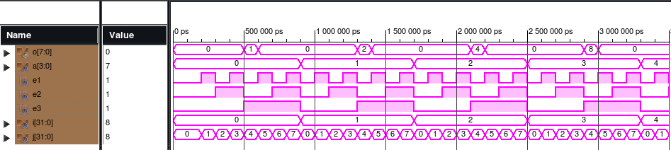
Decoder example
Note that I made the outputs active-high, whereas the 138's outputs are active-low.
// decoder.v

`timescale 1ns / 1ps
`default_nettype none

module decoder
(
    input  wire       e1, e2, e3,
    input  wire [2:0] a,
    output wire [7:0] o
);
    // Selected output is HIGH if E3 & not E2 & not E1; else LOW
    wire e = e3 & ~e2 & ~e1;
    // Drive selected output to 'e'; others to LOW
    assign o[0] = (a==0 ? e : 0);
    assign o[1] = (a==1 ? e : 0);
    assign o[2] = (a==2 ? e : 0);
    assign o[3] = (a==3 ? e : 0);
    assign o[4] = (a==4 ? e : 0);
    assign o[5] = (a==5 ? e : 0);
    assign o[6] = (a==6 ? e : 0);
    assign o[7] = (a==7 ? e : 0);
    // Note that I made the outputs active high here,
    // whereas the 74LS138 outputs are active low
endmodule
Test bench.
// decoder_tb.v

`timescale 1ns / 1ps
`default_nettype none

module decoder_tb;
    // Inputs for decoder
    reg  [3:0] a=0;
    reg        e1=0, e2=0, e3=0;
    // Outputs of decoder
    wire [7:0] o;

    // Instantiate the Unit Under Test (UUT)
    decoder uut
    (
        .a(a), .e1(e1), .e2(e2), .e3(e3),
        .o(o)
    );

   integer i=0, j=0;
   initial begin
	#100;  // Wait 100 ns for simulator reset to finish
	for (i=0; i<8; i=i+1) begin
	    for (j=0; j<8; j=j+1) begin
		a = i;
		{e3,e2,e1} = j;
		#100;  // Wait 100 ns so that we can see output update
	    end
	end
	$finish;
    end
endmodule
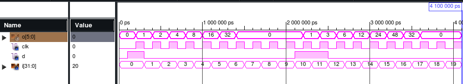
Shift register example
Note Verilog syntax for synchronous logic: always @ (posedge clk)
// shiftreg.v

`timescale 1ns / 1ps
`default_nettype none

module shiftreg
(
    input  wire       clk,
    input  wire       d,
    output wire [5:0] o
);
    reg [5:0] oreg=0;
    always @ (posedge clk) begin
        oreg[5] <= oreg[4];
        oreg[4] <= oreg[3];
        oreg[3] <= oreg[2];
        oreg[2] <= oreg[1];
        oreg[1] <= oreg[0];
        oreg[0] <= d;
    end
    assign o = oreg;
endmodule
Test bench.
// shiftreg_tb.v

`timescale 1ns / 1ps
`default_nettype none

module shiftreg_tb;
    // Inputs for shiftreg
    reg        clk=0, d=0;
    // Outputs of shiftreg
    wire [5:0] o;

    // Instantiate the Unit Under Test (UUT)
    shiftreg uut
    (
        .clk(clk), .d(d),
        .o(o)
    );

   integer i=0;
   initial begin
	#100;  // Wait 100 ns for simulator reset to finish
	for (i=0; i<20; i=i+1) begin
            // Send in a short pulse at i=0 and a longer pulse at i=10
            d = (i==0 || i==10 || i==11);
	    #100;  // Wait 100 ns, jiggle the clock, and wait another 100 ns
            clk = 1;
	    #100;
            clk = 0;
	end
	$finish;
    end
endmodule
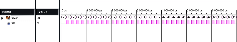
Counter example
// counter.v

`timescale 1ns / 1ps
`default_nettype none

module counter
(
    input  wire       clk,
    output wire [5:0] o
);
    reg [5:0] oreg=0;
    always @ (posedge clk) begin
        oreg <= oreg+1;
    end
    assign o = oreg;
endmodule
Test bench.
// counter_tb.v

`timescale 1ns / 1ps
`default_nettype none

module counter_tb;
    // Inputs for counter
    reg        clk=0;
    // Outputs of counter
    wire [5:0] o;

    // Instantiate the Unit Under Test (UUT)
    counter uut
    (
        .clk(clk),
        .o(o)
    );

   integer i=0;
   initial begin
	#100;  // Wait 100 ns for simulator reset to finish
	for (i=0; i<100; i=i+1) begin
	    #100;  // Wait 100 ns, jiggle the clock, and wait another 100 ns
            clk = 1;
	    #100;
            clk = 0;
	end
	$finish;
    end
endmodule
Lab
Part 1
- I have combined several of the example programs from lecture into a single Verilog design file, lab9.v. Download this file as well as lab9_tb.v (Verilog test bench), lab9.ucf (Xilinx pin assignments), and lab9.xise (Xilinx project file) from http://positron.hep.upenn.edu/p364/lab9
- Start up Xilinx ISE on your lab computer, open lab9.xise, compile, simulate.
- Once this works, plug your FPGA board into your breadboard.
- Notes about power, etc.
- Notes about logic levels.
- Notes about having only 12 of these to last us the rest of the semester.
- I have pre-programmed the lab9 project into your FPGA
- Pins 2 and 3 are the A and B inputs for the NAND, AND, OR, and XOR gates; pin 2 is the A input for the inverter.
- Pin 22 is the inverter output: NOT A.
- Pin 23 is the NAND output: A NAND B.
- Pin 24 is the AND output: A AND B.
- Pin 25 is the OR output: A OR B.
- Pin 26 is the XOR output: A XOR B.
- For the four-bit full adder, pin 4 is Cin; pins 10,11,12,13 are A0,A1,A2,A3; pins 14,15,16,17 are B0,B1,B2,B3; pins 27,28,29,30 are Sum0,Sum1,Sum2,Sum3; pin 31 is Cout.
- For the decoder, pins 32,33,34,35,36,37,38,39 are O0-O7; pins 2,3,4 are re-used for A0-A2; and pin 1 is an active-high enable.
- Note that all of this stuff together uses up about 30% of the logic cells in the chip (see fitter report after you compile) -- and this is one of the smallest Xilinx chips available
/*
 * lab9.v
 * Skeletal program from which to begin PHYS364 Lab 9
 * begun 2010-11-04 by Bill Ashmanskas, ashmansk@hep.upenn.edu
 */

`timescale 1ns / 1ps
`default_nettype none


module lab9
(
   /*
    * I chose these dumb names for the I/O signals
    * so that the mapping to pin numbers on the CMOD
    * DIP package is obvious.  Normally you would
    * give the I/O pins mnemonic names and would put
    * them into the .ucf file accordingly.
    */
    input  wire pin01, pin02, pin03, pin04,
    input  wire pin09, pin10, pin11, pin12, pin13,
    input  wire pin14, pin15, pin16, pin17, pin18,
    output wire pin22, pin23, pin24, pin25, pin26,
    output wire pin27, pin28, pin29, pin30, pin31,
    output wire pin32, pin33, pin34, pin35, pin36,
    output wire pin37, pin38, pin39, pin40
);
    nand_etc nand_etc_instance (
        .a(pin02), .b(pin03),
	.not_a(pin22), .a_nand_b(pin23),
	.a_and_b(pin24), .a_or_b(pin25), .a_xor_b(pin26));
    fourbit_fulladder fourbit_fulladder_instance (
        .cin(pin04),
        .a({pin13,pin12,pin11,pin10}),
        .b({pin17,pin16,pin15,pin14}),
	.sum({pin30,pin29,pin28,pin27}), .cout(pin31));
    decoder decoder_instance (
        .e1(0), .e2(0), .e3(pin01), .a({pin04,pin03,pin02}),
	.o({pin39,pin38,pin37,pin36,pin35,pin34,pin33,pin32}));
endmodule


module nand_etc
(
    input  wire a,
    input  wire b,
    output wire not_a,
    output wire a_nand_b,
    output wire a_and_b,
    output wire a_or_b,
    output wire a_xor_b
);
    assign not_a    = ~a;
    assign a_nand_b = ~(a&b);
    assign a_and_b  = a&b;
    assign a_or_b   = a|b;
    assign a_xor_b  = a^b;
endmodule


module fourbit_fulladder
(
    input  wire       cin,
    input  wire [3:0] a,
    input  wire [3:0] b,
    output wire [3:0] sum,
    output wire       cout
);
    assign {cout,sum} = a+b+cin;
endmodule


module decoder
(
    input  wire       e1, e2, e3,
    input  wire [2:0] a,
    output wire [7:0] o
);
    // Selected output is HIGH if E3 & not E2 & not E1; else LOW
    wire e = e3 & ~e2 & ~e1;
    // Drive selected output to 'e'; others to LOW
    assign o[0] = (a==0 ? e : 0);
    assign o[1] = (a==1 ? e : 0);
    assign o[2] = (a==2 ? e : 0);
    assign o[3] = (a==3 ? e : 0);
    assign o[4] = (a==4 ? e : 0);
    assign o[5] = (a==5 ? e : 0);
    assign o[6] = (a==6 ? e : 0);
    assign o[7] = (a==7 ? e : 0);
    // Note that I made the outputs active high here,
    // whereas the 74LS138 outputs are active low
endmodule
# lab9.ucf -- mapping Verilog names to FPGA pins

NET "pin01"  LOC="12" | IOSTANDARD=LVTTL ;
NET "pin02"  LOC="13" | IOSTANDARD=LVTTL ;
NET "pin03"  LOC="14" | IOSTANDARD=LVTTL ;
NET "pin04"  LOC="16" | IOSTANDARD=LVTTL ;
NET "pin09"  LOC="18" | IOSTANDARD=LVTTL ;
NET "pin10"  LOC="19" | IOSTANDARD=LVTTL ;
NET "pin11"  LOC="20" | IOSTANDARD=LVTTL ;
NET "pin12"  LOC="21" | IOSTANDARD=LVTTL ;
NET "pin13"  LOC="22" | IOSTANDARD=LVTTL ;
NET "pin14"  LOC="23" | IOSTANDARD=LVTTL ;
NET "pin15"  LOC="27" | IOSTANDARD=LVTTL ;
NET "pin16"  LOC="28" | IOSTANDARD=LVTTL ;
NET "pin17"  LOC="29" | IOSTANDARD=LVTTL ;
NET "pin18"  LOC="30" | IOSTANDARD=LVTTL ;
NET "pin22"  LOC="31" | IOSTANDARD=LVTTL ;
NET "pin23"  LOC="32" | IOSTANDARD=LVTTL ;
NET "pin24"  LOC="33" | IOSTANDARD=LVTTL ;
NET "pin25"  LOC="34" | IOSTANDARD=LVTTL ;
NET "pin26"  LOC="36" | IOSTANDARD=LVTTL ;
NET "pin27"  LOC="37" | IOSTANDARD=LVTTL ;
NET "pin28"  LOC="38" | IOSTANDARD=LVTTL ;
NET "pin29"  LOC="39" | IOSTANDARD=LVTTL ;
NET "pin30"  LOC="40" | IOSTANDARD=LVTTL ;
NET "pin31"  LOC="41" | IOSTANDARD=LVTTL ;
NET "pin32"  LOC="42" | IOSTANDARD=LVTTL ;
NET "pin33"  LOC="43" | IOSTANDARD=LVTTL ;
NET "pin34"  LOC="44" | IOSTANDARD=LVTTL ;
NET "pin35"  LOC="1"  | IOSTANDARD=LVTTL ;
NET "pin36"  LOC="2"  | IOSTANDARD=LVTTL ;
NET "pin37"  LOC="3"  | IOSTANDARD=LVTTL ;
NET "pin38"  LOC="5"  | IOSTANDARD=LVTTL ;
NET "pin39"  LOC="6"  | IOSTANDARD=LVTTL ;
NET "pin40"  LOC="8"  | IOSTANDARD=LVTTL ;
Part 2
- Now load lab9_synchronous.v, which includes the counter and the shift register shown in lecture today.
- Compile it, simulate it, load it into your FPGA, make it display to a bank of LEDs. (Probably the block of 10 LEDs in a DIP package is easiest to wire up.)
- Now modify the program so that the counter shows its output on a 7-segment LED display.
- pin 1 = lower left; pin 2 = bottom; pin 4 = lower right; pin 6 = upper right; pin 7 = top; pin 9 = upper left; pin 10 = center; pin 3 = common LED positive line.
- Now modify the program so that the counter adds a 4-bit number (programmed with DIP switch bank) each cycle instead of just adding 1.
- Show that it works for counting up by 1, 2, 3. Does it stop when you count up by zero?
- What value do you set on the switches to make the counter count down by ones? Down by twos?
/*
 * lab9_synchronous.v
 * Skeletal program from which to begin PHYS364 Lab 9 (part 2)
 * begun 2010-11-04 by Bill Ashmanskas, ashmansk@hep.upenn.edu
 */

`timescale 1ns / 1ps
`default_nettype none


module lab9_synchronous
(
   /*
    * I chose these dumb names for the I/O signals
    * so that the mapping to pin numbers on the CMOD
    * DIP package is obvious.  Normally you would
    * give the I/O pins mnemonic names and would put
    * them into the .ucf file accordingly.
    */
    input  wire pin01, pin02, pin03, pin04,
    input  wire pin09, pin10, pin11, pin12, pin13,
    input  wire pin14, pin15, pin16, pin17, pin18,
    output wire pin22, pin23, pin24, pin25, pin26,
    output wire pin27, pin28, pin29, pin30, pin31,
    output wire pin32, pin33, pin34, pin35, pin36,
    output wire pin37, pin38, pin39, pin40
);
    counter counter_instance (
        .clk(pin01),
        .o({pin40,pin39,pin38,pin37,pin36,pin35}));
    shiftreg shiftreg_instance (
	.clk(pin01), .d(pin02),
        .o({pin34,pin33,pin32,pin31,pin30,pin29}));
endmodule


module counter
(
    input  wire       clk,
    output wire [5:0] o
);
    reg [5:0] oreg=0;
    always @ (posedge clk) begin
        oreg <= oreg+1;
    end
    assign o = oreg;
endmodule


module shiftreg
(
    input  wire       clk,
    input  wire       d,
    output wire [5:0] o
);
    reg [5:0] oreg=0;
    always @ (posedge clk) begin
        oreg[5] <= oreg[4];
        oreg[4] <= oreg[3];
        oreg[3] <= oreg[2];
        oreg[2] <= oreg[1];
        oreg[1] <= oreg[0];
        oreg[0] <= d;
    end
    assign o = oreg;
endmodule
Part 3
- Modify the shift register in lab9_synchronous.v so that it requires no input (except the 1Hz clock). Instead:
- on each clock cycle, bits 1,2,3,4,5 take on the old values of bits 0,1,2,3,4;
- if all bits were zero, bit 0 gets a one; otherwise, bit 0 gets a zero
- else move every bit to the right by one place and put a zero
- Display the output on your rectangular bank of LEDs
- Now re-wire the output so that the 7-segment LED display rotates through these six states: