User:Ashmanskas/p364/2012/lab11c
From LaPET electronics
< User:Ashmanskas | p364 | 2012
Contents |
PHYS 364, fall 2012, lab 11c
- i.e. day three of Lab #11: Wednesday, Nov 28
- Here is a link to last week's lab: lab11.pdf
- Here is a link to last week's reading: reading11.pdf
- Here is a link to Monday's lab: lab11b
- Here is a link to today's reading: reading11b.pdf
- Xilinx "user constraint file" from last time: basys2.ucf
- Last Verilog program from last time: lab11b.v
- Last Xilinx programming file from last time: lab11b_part3.bit
- There is no lab report required, but at the end of the day, you should email your Verilog code to ashmansk@hep.upenn.edu. If you worked with a lab partner, be sure to CC him or her on your email so that I know that your submission is for two people.
Part 1
- Let's start from where we left off on Monday. We put together eight D-type flip-flops (with enable pins) to make an 8-bit counter, whose Q values were displayed on the green LEDs of the BASYS2 board.
- Several people pointed out that it was a bit of a pain to have to clock the counter by hand. Let's fix that!
- The BASYS2 board includes a 25 MHz on-board clock, which is wired to the mclk input of the FPGA.
- 25 MHz is a good speed for a serious electronics project, but it's too fast for us to see what's happening while we're just learning about digital circuits. Let's find a way to slow it down to a more reasonable speed.
- Suppose that you clocked your 8-bit counter from last time at frequency f = 1 Hz. Then bit 0 of the counter would toggle at f/2, bit 1 would toggle at f/4, ..., and bit 7 would toggle at f/256. For this reason, a single D-type flip flop whose D input is connected to the NOT of its Q output is called a "divide by two," because it is effectively dividing the clock frequency in half. The 8-bit counter divides the clock frequency by 256.
- Let's make a 17-bit counter to divide 25 MHz down to about 191 Hz, which will let us build circuits whose effects we can begin to see with our eyes.
- Now the result is that bit 7 of your 8-bit counter (which is connected to LED7 on the board) blinks with a period of 1.34 seconds.
//
// lab11c.v
// Verilog source code for Lab 11c (part 1)
// PHYS 364, UPenn, fall 2012
//

`default_nettype none

module lab11c
  (
   input        mclk,  // 25 MHz clock built into the BASYS2 board
   output [6:0] seg,   // red 7-segment display to draw numbers & letters
   output       dp,    // decimal point for 7-seg (0=ON, 1=OFF)
   output [3:0] an,    // shared LED anode signal per 7-seg digit (0=ON)
   output [7:0] led,   // 8 green LEDs, just above sliding switches
   input  [7:0] sw,    // 8 sliding switches (up=1, down=0)
   input  [3:0] btn,   // 4 push buttons (normal=0, pushed=1)
   input  [4:1] ja,    // 4 pins (JA, NW corner) can connect to breadboard
   input  [4:1] jb,    // 4 pins (JB) can connect to breadboard
   input  [4:1] jc,    // 4 pins (JC) can connect to breadboard
   input  [4:1] jd     // 4 pins (JD, NE corner) can connect to breadboard
   );

    // This counter will count 0..131071 over and over again,
    // using the 25 MHz on-board oscillator as its clock input
    wire [16:0] count17bit;
    counter_17bit mycounter1 (count17bit, mclk);

    // Now we can use bit 16 of the clock to get a frequency
    // (25 MHz) / (131072) = 190.7 Hz
    wire clk191Hz = count17bit[16];

    // We will use the 'Q' output of the SR latch as a clock
    // for the counter's flip-flops, so that we can clock the
    // counter by hand, one clock cycle at a time.
    // Now instead of using the 'Q' output of the SR latch as
    // a clock for the 8-bit counter's flip-flops, let's use
    // our new 191 Hz clock instead.
    wire clock = clk191Hz;

    // The rest of this module is the same as it was at the end of
    // Monday's lab.

    // Now we set up 8 D-type flip-flops that have an additional
    // input wire called ENABLE.  If ENABLE is TRUE, then the
    // flip-flop behaves exactly as an ordinary DFF.  But if ENABLE
    // is FALSE, then the DFF does nothing.

    // Now we connect each flip flop's D input to the NOT of its own
    // Q output.  So if ENABLE is asserted, the flip-flop just toggles
    // back and forth between 0 and 1.  But if ENABLE is deasserted,
    // the flip-flop does nothing.
    wire q7, q6, q5, q4, q3, q2, q1, q0;
    wire d7 = ~q7;
    wire d6 = ~q6;
    wire d5 = ~q5;
    wire d4 = ~q4;
    wire d3 = ~q3;
    wire d2 = ~q2;
    wire d1 = ~q1;
    wire d0 = ~q0;

    // Here is the tricky part:  the first flip flop is always enabled.
    // The second flip flop is only enabled if the first one is HIGH.
    // The third flip flop is only enabled if the first two are HIGH.
    // The fourth is only enabled if the first three are HIGH.  Etc.
    wire e0 = 1;
    wire e1 = q0;
    wire e2 = q0 & q1;
    wire e3 = q0 & q1 & q2;
    wire e4 = q0 & q1 & q2 & q3;
    wire e5 = q0 & q1 & q2 & q3 & q4;
    wire e6 = q0 & q1 & q2 & q3 & q4 & q5;
    wire e7 = q0 & q1 & q2 & q3 & q4 & q5 & q6;
    dffe mydff0 (q0, clock, d0, e0);
    dffe mydff1 (q1, clock, d1, e1);
    dffe mydff2 (q2, clock, d2, e2);
    dffe mydff3 (q3, clock, d3, e3);
    dffe mydff4 (q4, clock, d4, e4);
    dffe mydff5 (q5, clock, d5, e5);
    dffe mydff6 (q6, clock, d6, e6);
    dffe mydff7 (q7, clock, d7, e7);

    // Display the 8 flip flops' Q values on the 8 green LEDs.
    assign led[7] = q7;
    assign led[6] = q6;
    assign led[5] = q5;
    assign led[4] = q4;
    assign led[3] = q3;
    assign led[2] = q2;
    assign led[1] = q1;
    assign led[0] = q0;

   // These outputs are currently unused, but I connect them anyway to
   // keep the compiler from complaining.
    assign seg[6:0] = 0;
    assign dp = 0;
    assign an[3:0] = ~btn[3:0];
endmodule


module counter_17bit (output [16:0] q, input clk);
    wire [16:0] enable;
    assign enable[ 0] = 1;
    assign enable[ 1] = q[0];
    assign enable[ 2] = q[ 1:0]=='b11;
    assign enable[ 3] = q[ 2:0]=='b111;
    assign enable[ 4] = q[ 3:0]=='b1111;
    assign enable[ 5] = q[ 4:0]=='h1f;
    assign enable[ 6] = q[ 5:0]=='h3f;
    assign enable[ 7] = q[ 6:0]=='h7f;
    assign enable[ 8] = q[ 7:0]=='hff;
    assign enable[ 9] = q[ 8:0]=='h1ff;
    assign enable[10] = q[ 9:0]=='h3ff;
    assign enable[11] = q[10:0]=='h7ff;
    assign enable[12] = q[11:0]=='hfff;
    assign enable[13] = q[12:0]=='h1fff;
    assign enable[14] = q[13:0]=='h3fff;
    assign enable[15] = q[14:0]=='h7fff;
    assign enable[16] = q[15:0]=='hffff;
    // Every 'D' input is the NOT of the corresponding 'Q' output
    wire [16:0] d = ~q[16:0];
    dffe mydff0  (q[ 0], clk, d[ 0], enable[0]);
    dffe mydff1  (q[ 1], clk, d[ 1], enable[1]);
    dffe mydff2  (q[ 2], clk, d[ 2], enable[2]);
    dffe mydff3  (q[ 3], clk, d[ 3], enable[3]);
    dffe mydff4  (q[ 4], clk, d[ 4], enable[4]);
    dffe mydff5  (q[ 5], clk, d[ 5], enable[5]);
    dffe mydff6  (q[ 6], clk, d[ 6], enable[6]);
    dffe mydff7  (q[ 7], clk, d[ 7], enable[7]);
    dffe mydff8  (q[ 8], clk, d[ 8], enable[8]);
    dffe mydff9  (q[ 9], clk, d[ 9], enable[9]);
    dffe mydff10 (q[10], clk, d[10], enable[10]);
    dffe mydff11 (q[11], clk, d[11], enable[11]);
    dffe mydff12 (q[12], clk, d[12], enable[12]);
    dffe mydff13 (q[13], clk, d[13], enable[13]);
    dffe mydff14 (q[14], clk, d[14], enable[14]);
    dffe mydff15 (q[15], clk, d[15], enable[15]);
    dffe mydff16 (q[16], clk, d[16], enable[16]);
endmodule


// This magic incantation is how you tell the Xilinx compiler to make
// a D-type flip-flop with the ENABLE feature.
module dffe (output q, input clk, input d, input enable);
    reg q_reg;
    always @ (posedge clk) if (enable) q_reg <= d;
    assign q = q_reg;
endmodule


// This module implements the SR latch that we studied in Reading #11.
// You draw two NOR gates.  The output of the first NOR gate is called
// 'q'.  The output of the second NOR gate is called 'qbar' (i.e. the
// opposite of 'q').  The first NOR gate's inputs are connected to r
// (reset) and qbar.  The second NOR gate's inputs are connected to s
// (set) and q.  Normally, neither r nor s is asserted, and q keeps
// its previous state.  If you assert r (but not s), then q goes to 0.
// If you assert s (but not r), then q goes to 1.  An undefined state
// results if r and s are asserted together.
module srlatch (output q, input s, input r);
    // We define the wire 'qbar' here, but we don't connect it to
    // anything, because using it as the output argument of the second
    // nor_gate will connect it.  You can see that the wire called
    // 'qbar' connects the output of the second NOR gate to an input
    // of the first NOR gate, just as you would do if you were drawing
    // a schematic diagram of an SR latch.
    wire qbar;
    nor mynorgate1 (qbar, q, s);
    nor mynorgate2 (q, qbar, r);
endmodule
- Compile the above program, load it into your board, and verify that LED7 blinks with a period of about 1.34 seconds (i.e. check visually that it is a little bit slower than 1 Hz).
- Now let's try a slightly different way of making an 8-bit counter. First, we'll define a module called dffe_8bit, which will make an 8-bit version of a D-type flip-flop. Add this module to the bottom of your Verilog file:
// Implement an 8-bit D-type flip-flop, with 'enable' and 'reset' inputs
module dffe_8bit (output [7:0] q, input clk, input [7:0] d,
                  input enable, input reset);
    // if 'reset' is asserted, then the data input to the eight
    // flip-flops will be all zeros; otherwise, the data input
    // will just be d[7:0]
    wire [7:0] data = (reset ? 0 : d[7:0]);
    dffe mydff0 (q[0], clk, data[0], enable);
    dffe mydff1 (q[1], clk, data[1], enable);
    dffe mydff2 (q[2], clk, data[2], enable);
    dffe mydff3 (q[3], clk, data[3], enable);
    dffe mydff4 (q[4], clk, data[4], enable);
    dffe mydff5 (q[5], clk, data[5], enable);
    dffe mydff6 (q[6], clk, data[6], enable);
    dffe mydff7 (q[7], clk, data[7], enable);
endmodule
- Now replace the last few dozen lines of the main lab11c module (starting from just below the wire clock = clk191Hz; line, and ending with the first endmodule line) with this code:
    // The rest of this module WAS the same as it was at the end of
    // Monday's lab BUT WE ARE REPLACING IT NOW

    // Use 8-bit-wide D-type flip-flop to make an 8-bit counter

    // The 'enable' is controlled by a sliding switch
    wire slowcount_enable = !sw[0];

    // A push-button can 'reset' the counter back to zero
    wire slowcount_reset = btn[0];

    // These wires hold the current counter value
    wire [7:0] slowcount;

    // These wires hold the next value to be loaded into the counter
    wire [7:0] slowcount_nextvalue = slowcount+1;

    // Instantiate the 8-bit-wide flip-flop
    dffe_8bit mydffe8bit1 (slowcount[7:0],       // Q outputs
			   clk191Hz,             // clock input
			   slowcount_nextvalue,  // D inputs
			   slowcount_enable,     // 'enable' input
			   slowcount_reset);     // 'reset' input

    // Display the 8 flip flops' Q values on the 8 green LEDs.
    assign led[7:0] = slowcount[7:0];

   // These outputs are currently unused, but I connect them anyway to
   // keep the compiler from complaining.
    assign seg[6:0] = 0;
    assign dp = 0;
    assign an[3:0] = ~btn[3:0];
endmodule
- By defining an 8-bit-wide flip-flop, we can make a counter with much less hassle. On each new clock cycle, the D[7:0] inputs for the flip-flop are just given by the new value (Q[7:0]+1). We can do this because, as we saw in last night's reading, Verilog knows how to express the addition of two integers in terms of the corresponding logic gates.
- Recompile this new program and load it into your board. Check that it still counts, with the slowest LED blinking a bit slower than 1 Hz.
- Also, check that when you slide one of the switches (which one?) to a certain position (what position?), the counter stops counting. It resumes counting when you slide the switch back.
- Also, check that when you press one of the buttons (which one?), the counter is "reset" back to zero.
- Can you see how all of this works inside the Verilog code?
- Can you envision what the internal schematic diagram for all of this would look like, if built up out of individual logic gates? (Don't try too hard at this. Just try to imagine vaguely how the Verilog turns into logic gates.)
Part 2
- Modify your program from Part 1 so that LED7 blinks at 1.00 Hz, i.e. get the frequency to within about a percent of exactly 1 Hz.
- Here is a hint: modify the rule for the next value that the slow counter will take.
- If the current value of the counter is 190, you want the next value to be 0;
- otherwise, you want the next value to be the current value plus one, as it is now.
- You can achieve this using the "ternary operator" from the reading, i.e. the expression (condition ? valueA : valueB)
- Compile your program, load it into the board, and check that you get a frequency of 1 Hz from LED7.
- Now define a new wire called clk1Hz and connect it to bit 7 of your "slow" counter, like this: wire clk1Hz = slowcounter[7];
- Now let's use this clk1Hz signal as the clock for another 8-bit counter, so that it will count up at a frequency of one hertz: one mississippi, two mississippi, three mississippi, etc.
- The code should look something like this (just below the code that instantiates mydffe8bit1):
- Remember not to assign the led[7:0] outputs twice. The last line replaces the existing LED assignment.
    // Make a new clock that ticks at just 1 Hz
    wire clk1Hz = slowcount[7];
    // Make a new counter that counts at 1 Hz
    wire [7:0] count1Hz;
    wire [7:0] count1Hz_next = count1Hz+1;
    dffe_8bit mydffe8bit2 (count1Hz[7:0],        // Q outputs
			   clk1Hz,               // clock input
			   count1Hz_next[7:0],   // D inputs
			   1,                    // 'enable' input
			   btn[1]);              // 'reset' input
    // Display the VERY slow counter on the 8 green LEDs.
    assign led[7:0] = count1Hz[7:0];
Part 3
- Now let's display the lowest 4 bits of count1Hz on the 7-segment LED display.
- The connections for the 7-segment display look something like this image from the BASYS2 reference manual:
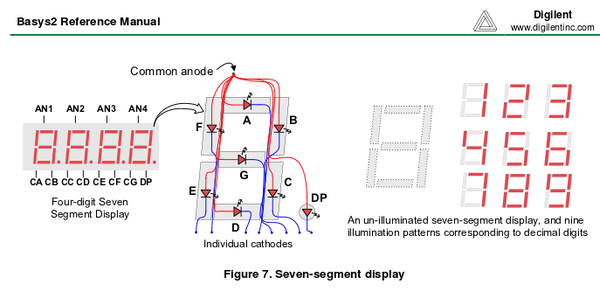
- The top segment ("A" on the diagram) is driven by led[0]. The upper-right segment (B) is driven by led[1]. And so on for C, D, E, F, G.
- Also, it turns out that assign led[0] = 1; turns OFF the top segment, and assign led[3] = 0; turns ON the bottom segment, etc. This is because the FPGA outputs are connected to the lower-voltage sides (cathodes) of the diodes, not the higher-voltage sides (anodes). The higher-voltage sides (anodes) are connected to the an[3:0] FPGA pins, in a way that we will see below.
- Modify the assignment for an[3:0] to this (I'll explain below):
assign an[3] = slowcount[6:5]!=3;
assign an[2] = slowcount[6:5]!=2;
assign an[1] = slowcount[6:5]!=1;
assign an[0] = slowcount[6:5]!=0;
- Also modify the bottom dozen or so lines of the lab11c module (starting from assign led[7:0] = count1Hz[7:0];) so that they look like this:
    // Digit will display low 4 bits of the very slow counter
    wire [3:0] digit = count1Hz[3:0];

    // Create wires that are '1' when corresponding segment is ON
    wire [6:0] seg_is_on;
    assign seg_is_on[0] = (digit==0)   || (digit==2)   || (digit==3)   ||
			  (digit==5)   || (digit==6)   || (digit==7)   ||
			  (digit==8)   || (digit==9)   || (digit=='hA) ||
			  (digit=='hC) || (digit=='hE) || (digit=='hF);
    // You need to fill in the answers for 1, 2, 3, 4, 5, 6
    assign seg_is_on[6:1] = 0;

    // Each LED actually lights up when 'seg' is LOW not HIGH
    assign seg[6:0] = ~seg_is_on[6:0];

    // We're not using the decimal point now, so just light it up
    assign dp = 0;

    // This is the mysterious anode wiring ?!
    assign an[3] = slowcount[6:5]!=3;
    assign an[2] = slowcount[6:5]!=2;
    assign an[1] = slowcount[6:5]!=1;
    assign an[0] = slowcount[6:5]!=0;
endmodule
- I wrote the logic for you for seg_on[0]. You need to write your own logic for seg_on[1], seg_on[2], ..., seg_on[6].
- When you think you have it, compile the program and load it into your board!
