User:Ashmanskas/p364/2012/lab11d
From LaPET electronics
< User:Ashmanskas | p364 | 2012
Contents |
PHYS 364, fall 2012, lab 11d
- i.e. day four of Lab #11: Friday, Nov 30
- Here is a link to last week's lab: lab11.pdf
- Here is a link to last week's reading: reading11.pdf
- Here is a link to Monday's lab: lab11b
- Here is a link to Wednesday's lab: lab11c
- Here is a link to Wednesday's reading: reading11b.pdf
- Xilinx "user constraint file" from last time: basys2.ucf
- There is no lab report required, but at the end of the day, you should email your Verilog code to ashmansk@hep.upenn.edu. If you worked with a lab partner, be sure to CC him or her on your email so that I know that your submission is for two people.
- Over the weekend, I will email the next reading assignment, to be completed by the end of class on Monday (but preferably
before you come to class). It will be similar in length to the last reading — not too arduous.
Part 1
- Let's start from where we left off on Wednesday.
- It turns out that the explanation for everyone's 1 Hz clock initially ticking at 2 Hz is exactly what Jose suspected: the on-board oscillator on the BASYS2 board (which drives the 'mclk' input pin on the FPGA) is in fact a 50 MHz clock, while I had thought that it was a 25 MHz clock.
- I have written a module called display4digits, which takes four digits' worth of input bits and uses them to drive all four of the 7-segment displays.
- The updated Verilog file can be found here: lab11d.v
- The same code is listed here, in case you find it convenient:
//
// lab11d.v
// Verilog source code for Lab 11d (part 1)
// PHYS 364, UPenn, fall 2012
//
`default_nettype none
module lab11d
(
input mclk, // 50 MHz clock built into the BASYS2 board
output [6:0] seg, // red 7-segment display to draw numbers & letters
output dp, // decimal point for 7-seg (0=ON, 1=OFF)
output [3:0] an, // shared LED anode signal per 7-seg digit (0=ON)
output [7:0] led, // 8 green LEDs, just above sliding switches
input [7:0] sw, // 8 sliding switches (up=1, down=0)
input [3:0] btn, // 4 push buttons (normal=0, pushed=1)
input [4:1] ja, // 4 pins (JA, NW corner) can connect to breadboard
input [4:1] jb, // 4 pins (JB) can connect to breadboard
output [4:1] jc, // 4 pins (JC) can connect to breadboard
output [4:1] jd // 4 pins (JD, NE corner) can connect to breadboard
);
// It turns out that the on-board oscillator is really 50 MHz,
// while I thought it was 25 MHz. Kudos to Jose for pointing
// this out as the most plausible explanation, which I then
// verified with an oscilloscope.
// This counter will count 0..262144 over and over again,
// using the 50 MHz on-board oscillator as its clock input
wire [17:0] count18bit;
counter_18bit mycounter1 (count18bit, mclk);
// Now we can use bit 17 of the clock to get a frequency
// (50 MHz) / (262144) = 190.7 Hz
wire clk191Hz = count18bit[17];
// Now instead of using the 'Q' output of the SR latch as a clock
// for the 8-bit counter's flip-flops, we use our new 191 Hz clock.
wire clock = clk191Hz;
// Use 8-bit-wide D-type flip-flop to make an 8-bit counter
//
// The 'enable' is controlled by a sliding switch
wire slowcount_enable = !sw[0];
// A push-button can 'reset' the counter back to zero
wire slowcount_reset = btn[0];
// These wires hold the current counter value
wire [7:0] slowcount;
// These wires hold the next value to be loaded into the counter
wire [7:0] slowcount_nextvalue = (slowcount==190 ? 0 : slowcount+1);
// Instantiate the 8-bit-wide flip-flop
dffe_8bit mydffe8bit1 (slowcount[7:0], // Q outputs
clk191Hz, // clock input
slowcount_nextvalue, // D inputs
slowcount_enable, // 'enable' input
slowcount_reset); // 'reset' input
// Make a new clock that ticks at just 1 Hz
wire clk1Hz = slowcount[7];
// Make a new counter that counts at 1 Hz
wire [7:0] count1Hz;
wire [7:0] count1Hz_next = count1Hz+1;
dffe_8bit mydffe8bit2 (count1Hz[7:0], // Q outputs
clk1Hz, // clock input
count1Hz_next[7:0], // D inputs
1, // 'enable' input
btn[1]); // 'reset' input
// Display the VERY slow counter on the 8 green LEDs.
assign led[7:0] = count1Hz[7:0];
// Instantiate 'display4digits' module to drive 7-segment display
wire [3:0] digit0, digit1, digit2, digit3, dots; // each is a 4-bit vector
wire [1:0] count0123;
display4digits myd4d1 (seg[6:0], dp, // module outputs to drive the FPGA
an[3:0], // pins for 7-segment display
count0123[1:0], // 2-bit counter to ping-pong digits
digit0[3:0], // value to display on right digit
digit1[3:0], // each digit can display a
digit2[3:0], // 4-bit number in hexadecimal
digit3[3:0], // value to display on left digit
dots[3:0]); // what to send to the 4 'dp' dots
// Connect useful values to the inputs of 'myd4d1'
assign count0123[1:0] = slowcount[5:4];
assign digit0[3:0] = 1;
assign digit1[3:0] = 2;
assign digit2[3:0] = 3;
assign digit3[3:0] = 4;
assign dots[3:0] = btn[3:0];
// Note that I changed the four JC pins and the four JD pins from
// INPUTs to OUTPUTs for today, so that we can use them to drive
// LEDs for the traffic-signal display in parts 2 and 3. Also
// notice that a 4-bit-wide Verilog vector does not necessarily
// have to number its four wires [3:0]. In this case, Digilent
// decided to number these four wires [4:1], and I decided to
// stick with their convention for these pins.
assign jc[4] = sw[7];
assign jc[3] = sw[6];
assign jc[2] = sw[5];
assign jc[1] = sw[4];
assign jd[4] = sw[3];
assign jd[3] = sw[2];
assign jd[2] = sw[1];
assign jd[1] = sw[0];
endmodule
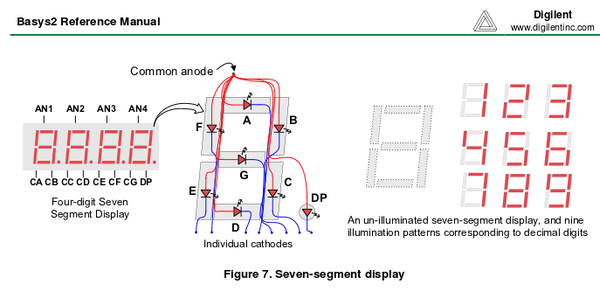
// This module drives the FPGA outputs ('seg', 'dp', 'an') that connect
// to the 4-digit 7-segment LED display. The display actually contains
// 32 separate LEDs (7 segments plus decimal, for each of 4 digits), but
// uses just 12 FPGA pins to drive them. The trick is to illuminate only
// one of the four digits at a time, but to alternate between the four
// digits so quickly that the human eye doesn't notice. The wire 'an[i]'
// connects to the anodes (positive sides) of all 8 LEDs on segment #i,
// while the wire 'seg[j]' connects to the cathodes (negative sides) of
// segment #j for all four digits. The 'dp' wire connects to the cathodes
// of all four decimal points.
module display4digits(output [6:0] seg, // 7-segment LED cathodes
output decimalpoint, // decimal-point cathodes
output [3:0] anode, // one anode per LED digit
input [1:0] count0123, // which digit to light up now
input [3:0] digit0, // bits for right-hand digit
input [3:0] digit1, // each digit value goes
input [3:0] digit2, // from 0 to F (hexadecimal)
input [3:0] digit3, // bits for left-hand digit
input [3:0] dots); // inputs for 4 DP dots
assign decimalpoint = (count0123==0) ? ~dots[0] :
(count0123==1) ? ~dots[1] :
(count0123==2) ? ~dots[2] : ~dots[3];
// Each digit's anode is driven HIGH (by an external PNP transistor)
// whenever the corresponding an[] bit is driven LOW by the FPGA; by
// illuminating one digit at a time in sequence, we can make all four
// digits appear to be always lit, but appearing to be displaying
// distinct digit values simultaneously
assign anode[0] = ~(count0123==0);
assign anode[1] = ~(count0123==1);
assign anode[2] = ~(count0123==2);
assign anode[3] = ~(count0123==3);
// We need to go ping-pong (4-way ping-pong) between the four input
// digits, to decide which digit we are currently converting into
// the corresponding 7 segments
wire [3:0] digit = (count0123==0) ? digit0 :
(count0123==1) ? digit1 :
(count0123==2) ? digit2 : digit3 ;
// Create wires that are '1' when corresponding segment is ON:
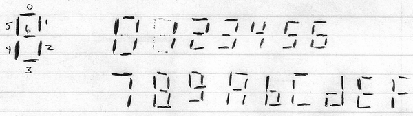
// seg 0=north, 1=NE, 2=SE, 3=south, 4=SW, 5=NW, 6=center
wire [6:0] seg_is_on =
// I thought you might enjoy this different way of decoding
// the numbers 0..F into the 7-segment ON/OFF pattern. But
// there is a bug here in the display of the 'F' digit: can
// you find a way to fix it?
(digit==0) ? 'b0111111 :
(digit==1) ? 'b0000110 :
(digit==2) ? 'b1011011 :
(digit==3) ? 'b1001111 :
(digit==4) ? 'b1100110 :
(digit==5) ? 'b1101101 :
(digit==6) ? 'b1111101 :
(digit==7) ? 'b0000111 :
(digit==8) ? 'b1111111 :
(digit==9) ? 'b1101111 :
(digit=='hA) ? 'b1110111 :
(digit=='hb) ? 'b1111100 :
(digit=='hC) ? 'b0111001 :
(digit=='hd) ? 'b1011110 :
(digit=='hE) ? 'b1111001 :
'b1000111 ;
// Each digit's corresponding LED segment lights up when its
// 'seg' bit is LOW, which drives that LED's cathode to ground
assign seg[6:0] = ~seg_is_on[6:0];
endmodule
module counter_18bit (output [17:0] q, input clk);
wire [17:0] enable;
// Each FF is enabled if all previous FFs have Q==1
assign enable[ 0] = 1;
assign enable[ 1] = q[0];
assign enable[ 2] = !(~q[ 1:0]); // the logical NOT of the bitwise NOT
assign enable[ 3] = !(~q[ 2:0]); // is a way to check that all of
assign enable[ 4] = !(~q[ 3:0]); // the bits are HIGH
assign enable[ 5] = !(~q[ 4:0]);
assign enable[ 6] = !(~q[ 5:0]);
assign enable[ 7] = !(~q[ 6:0]);
assign enable[ 8] = !(~q[ 7:0]);
assign enable[ 9] = !(~q[ 8:0]);
assign enable[10] = !(~q[ 9:0]);
assign enable[11] = !(~q[10:0]);
assign enable[12] = !(~q[11:0]);
assign enable[13] = !(~q[12:0]);
assign enable[14] = !(~q[13:0]);
assign enable[15] = !(~q[14:0]);
assign enable[16] = !(~q[15:0]);
assign enable[17] = !(~q[16:0]);
// Every 'D' input is the NOT of the corresponding 'Q' output
wire [17:0] d = ~q[17:0];
dffe mydff0 (q[ 0], clk, d[ 0], enable[0]);
dffe mydff1 (q[ 1], clk, d[ 1], enable[1]);
dffe mydff2 (q[ 2], clk, d[ 2], enable[2]);
dffe mydff3 (q[ 3], clk, d[ 3], enable[3]);
dffe mydff4 (q[ 4], clk, d[ 4], enable[4]);
dffe mydff5 (q[ 5], clk, d[ 5], enable[5]);
dffe mydff6 (q[ 6], clk, d[ 6], enable[6]);
dffe mydff7 (q[ 7], clk, d[ 7], enable[7]);
dffe mydff8 (q[ 8], clk, d[ 8], enable[8]);
dffe mydff9 (q[ 9], clk, d[ 9], enable[9]);
dffe mydff10 (q[10], clk, d[10], enable[10]);
dffe mydff11 (q[11], clk, d[11], enable[11]);
dffe mydff12 (q[12], clk, d[12], enable[12]);
dffe mydff13 (q[13], clk, d[13], enable[13]);
dffe mydff14 (q[14], clk, d[14], enable[14]);
dffe mydff15 (q[15], clk, d[15], enable[15]);
dffe mydff16 (q[16], clk, d[16], enable[16]);
dffe mydff17 (q[17], clk, d[17], enable[17]);
endmodule
// Implement an 8-bit D-type flip-flop, with 'enable' and 'reset' inputs
module dffe_8bit (output [7:0] q, input clk, input [7:0] d,
input enable, input reset);
// if 'reset' is asserted, then the data input to the eight
// flip-flops will be all zeros; otherwise, the data input
// will just be d[7:0]
wire [7:0] data = (reset ? 0 : d[7:0]);
dffe mydff0 (q[0], clk, data[0], enable);
dffe mydff1 (q[1], clk, data[1], enable);
dffe mydff2 (q[2], clk, data[2], enable);
dffe mydff3 (q[3], clk, data[3], enable);
dffe mydff4 (q[4], clk, data[4], enable);
dffe mydff5 (q[5], clk, data[5], enable);
dffe mydff6 (q[6], clk, data[6], enable);
dffe mydff7 (q[7], clk, data[7], enable);
endmodule
// This magic incantation is how you tell the Xilinx compiler to make
// a D-type flip-flop with the ENABLE feature.
module dffe (output q, input clk, input d, input enable);
reg q_reg;
always @ (posedge clk) if (enable) q_reg <= d;
assign q = q_reg;
endmodule
// This module implements the SR latch that we studied in Reading #11.
// You draw two NOR gates. The output of the first NOR gate is called
// 'q'. The output of the second NOR gate is called 'qbar' (i.e. the
// opposite of 'q'). The first NOR gate's inputs are connected to r
// (reset) and qbar. The second NOR gate's inputs are connected to s
// (set) and q. Normally, neither r nor s is asserted, and q keeps
// its previous state. If you assert r (but not s), then q goes to 0.
// If you assert s (but not r), then q goes to 1. An undefined state
// results if r and s are asserted together.
module srlatch (output q, input s, input r);
// We define the wire 'qbar' here, but we don't connect it to
// anything, because using it as the output argument of the second
// nor_gate will connect it. You can see that the wire called
// 'qbar' connects the output of the second NOR gate to an input
// of the first NOR gate, just as you would do if you were drawing
// a schematic diagram of an SR latch.
wire qbar;
nor mynorgate1 (qbar, q, s);
nor mynorgate2 (q, qbar, r);
endmodule
- Compile the above Verilog program and load it into your board. You should see 1234 displayed on the four digits of the 7-segment display.
- Carefully read through the comments in the new display4digits module and look again at the illustrations for how the 7-segment display is connected. See if you can understand how the FPGA manages to drive all four digits.
- Now make one small change to the assignment of count0123 in the top-level module (where it says "Connect useful values to the inputs of myd4d1") so that the FPGA alternates between the four different digits so quickly that your eye can't even detect the motion: make it update so quickly that it looks as if all four digits are displayed simultaneously.
- Hint: making it update about sixteen times as fast is a very easy way to do this.
- Recompile and see if '1234' now seem to be constantly illuminated.
- Now connect the digit0 ... digit3 inputs of the display4digits module so that the right-hand pair of digits displays the 8-bit counter that is ticking at 1 Hz (the same counter that drives the green LEDs), and so that the left-hand pair of digits displays the 8-bit value set by the eight sliding switches.
- When you load this into your board, you should see the right two digits ticking at 1 Hz.
- You should be able to manipulate the sliding switches to change the left two digits. But notice that sw[0] is still also connected to the slowcount_enable wire, so sliding that switch up will stop the clock, which stops all of the action.
- Notice that there is a bug in my logic for displaying the F digit to the 7-segment display.
- As I have it currently coded, the letter F displays backwards.
- Find and fix my bug, and make the letter F display correctly.
- Now that we have all four digits working correctly, we will make use of this display in Monday's lab.
Part 2
- So far, the things we have been able to do with logic gates and flip-flops have been pretty dull in comparison to the things that the Arduino can do.
- The way to make digital logic start to do things that begin to resemble the things that a computer can do is by implementing a finite-state machine (FSM).
- I am hoping that by the end of next week, we can figure out how to make an FSM that is sophisticated enough to give you some sense of how a real computer does its work.
- But we have to start somewhere, so let's start by designing a state machine to control a traffic signal.
- Here is a state diagram for a simple traffic light:
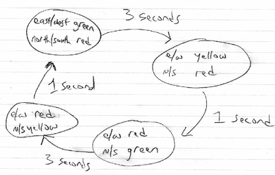
- Initially, the east/west traffic can go, and the north/south traffic is stopped.
- After a few seconds, the E/W light turns yellow.
- Then after just one second, the E/W light turns red, and the N/S light turns green.
- After a few seconds, the N/S light then turns yellow.
- Finally, after one more second, we return to the initial state.
- This is an absurdly fast traffic signal, but if we made it too realistic, it would be pretty boring to watch in the lab.
- Next week, we will see a more formal way to design a state machine, which is useful for complicated problems. But it turns out that the easiest way to implement a relatively simple FSM is just to use the value of a counter to tell you which state you are currently in.
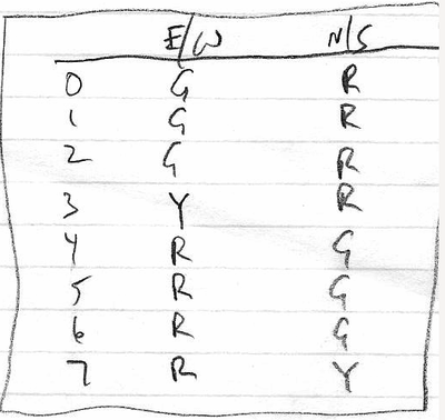
- The lowest 3 bits of count1Hz[7:0], in other words the vector count1Hz[2:0], will count over and over again from 0 to 7, updating once per second. This is just what we want.
- We can write something like wire [2:0] ticks = count1Hz[2:0]; and then use the value of ticks to control the traffic light display.
- Here is a possible mapping from the value of ticks to the state of the traffic signal:
- From the parts supply area, find your breadboard, six 100-ohm resistors, two red LEDs, two yellow LEDs, and two green LEDs, and one piece of breadboarding wire that is at least 10cm long.
- You don't need any external power for your breadboard. The BASYS2 board will provide all necessary power.
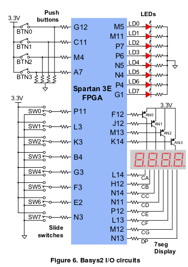
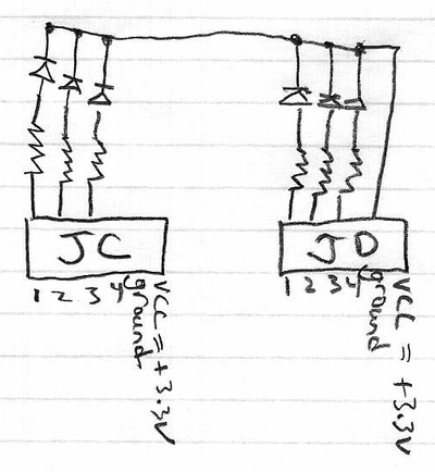
- At the top of the BASYS2 board are four 6-pin connectors for "user I/O" connections (in other words, your own inputs and outputs).
- From left to right, the four connectors are labeled JA, JB, JC, JD.
- From left to right, the pins of (for example) the right-hand connector are jd[1], jd[2], jd[3], jd[4], ground, Vcc, where "Vcc" means the +3.3 volt power that is used by the FPGA's input/output pins.
- A logic LOW output of an FPGA pin is 0.0 volts (ground).
- A logic HIGH output of an FPGA pin (for this FPGA) is +3.3 volts. (This is lower than the +5 volts used by the Arduino.)
- You want to wire up the six LEDs so that each LED lights up when the corresponding FPGA output pin is driven HIGH.
- I suggest using jc[1], jc[2], jc[3] for the north/south traffic signal, and using jd[1], jd[2], jd[3] for the east/west traffic signal. But it's up to you.
- Push one lead of a 100 ohm resistor into each of the connector holes corresponding to jc[1], jc[2], jc[3], jd[1], jd[2], jd[3], and push the other lead of each resistor into a separate column of your breadboard.
- Push one end of your 10cm length of breadboard wire into the "ground" hole for either the JC or the JD connector. (Note that "ground" is second from the end, while "Vcc" is on the end.)
- Wire up each LED in series with a resistor. Connect the negative end of each LED to the long "ground" strip of your breadboard. Connect the breadboard's ground to the BASYS2 board's ground with the breadboard wire.
- I have pre-wired the outputs jc[4:1] to sliding switches sw[7:4] and the outputs jd[4:1] to sliding switches sw[3:0] so that you can test out your LED connections before working on your Verilog program. Give them a try and make sure that they light up as you expect.
- Now assign each of the corresponding FPGA output pins to HIGH or LOW depending on the value of ticks in your Verilog code. For instance, the east/west yellow LED should only light up if (ticks==3) .
- Congratulations! You've just built a working traffic signal!
Part 3
- If you're not yet very comfortable with programming, then you may not reach this part of the lab today. That's OK — you can skip it if you run out of time.
- If you can at least get a good start on this part of the lab before time is up, please give it a try.
- The FSM from part 2 never has to change what it does in response to external input.
- A more interesting traffic signal would respond to the press of a WALK button.
- Let's add a WALK feature to our traffic light, like this:
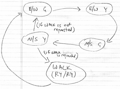
- Now there are two possible next states from the "north/south yellow" state: if there is a pedestrian waiting, then the next state should be WALK (where red/yellow together are illuminated for both N/S and E/W). If there is no pedestrian waiting, then the next state should be "east/west green."
- The easiest form of the "pedestrian waiting" signal is just to use a sliding switch, e.g. sw[7], even though a button would be nicer. (To use a button, you need to combine it with a set/reset latch, so that the button "sticks" until the next walk state has occurred.)
- Here is a straightforward way that we can use a 4-bit counter to include the walk phase of the light:
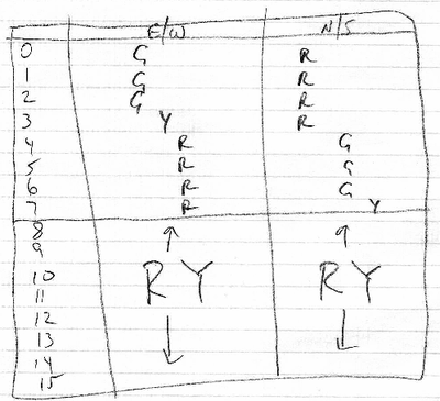
- To implement this, you need to change ticks from 3 bits to 4 bits, and update the LED logic to incorporate all 16 possible values of ticks. Note that you can use the less than ( < ) and greater than ( > ) operators in Verilog with integer values, or you can pick apart the bits of ticks[3:0] if you find that easier.
- You also need to change the logic for count1Hz_next. Instead of simply
wire [7:0] count1Hz_next = count1Hz + 1;
you need something like
wire [7:0] count1Hz_next = ((count1Hz==7 && !sw[7]) || (count1Hz==15)) ? 0 : count1Hz + 1;
- The result is that you go from ticks==7 to ticks==8 if the walk request sw[7] is HIGH, but you go from ticks==7 back to ticks==0 if the walk request is LOW. Also, you should go from count1Hz==15 back to count1Hz==0 so that you don't confuse yourself with the fact that count1Hz has 8 bits while ticks has only 4 bits.
- Really it was a bit inelegant of me to use separate names for count1Hz and for ticks. It makes things unnecessarily confusing.
- Extra credit: use an SR latch (the code for which is at the bottom of the Verilog file) that is SET when you push button #3 and is RESET when ticks[3] is HIGH. Now use the Q output of this SR latch for the walk request signal. Also, make one of the decimal point LEDs light up while the walk-requested signal is true, so that you can see that a walk has been requested.
