User:Ashmanskas/p364/2012/lab11e
From LaPET electronics
< User:Ashmanskas | p364 | 2012
PHYS 364, fall 2012, lab 11e
- i.e. day five of Lab #11: Monday, Dec 3
- Here is a link to the sort-of reading for today: fall 2010 lecture 10
- Here is a link to Friday's lab: lab11d
- Xilinx "user constraint file" from last time: basys2.ucf
- There is no lab report required, but at the end of the day, you should email your Verilog code (for part 2) to ashmansk@hep.upenn.edu. If you worked with a lab partner, be sure to CC him or her on your email so that I know that your submission is for two people.
Part 1
- This first part does not require you to do any programming, but there are some parts of my program that I want you to try to follow.
- Here is the Verilog file for part 1: lab11e_part1.v
- This time I'm not pasting the whole Verilog source file into this web page, because I don't want you to be overwhelmed by staring at 200 lines of program code all at once. There are only a few parts that you need to study.
- Make and compile an ISE project using the above Verilog file and the usual "user constraints" file basys2.ucf
- By the way, if you actually look through the basys2.ucf file in your web browser, you'll see that its main purpose is to assign human-usable names (like led, sw, btn, seg) to the FPGA's built-in input/output pins.
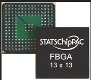
- The bottom of the FPGA looks something vaguely like the picture below. (This is not exactly the same pattern as the FPGA on your board, but it illustrates the same idea.)
- The UCF file contains lines that map the (row,column) pin names of the FPGA's physical package into mnemonic names that are easier to use inside your own logic circuit. For example:
# Pin assignment for DispCtl
# Connected to Basys2 onBoard 7seg display
NET "seg<0>" LOC = "L14"; # Bank = 1, Signal name = CA
NET "seg<1>" LOC = "H12"; # Bank = 1, Signal name = CB
NET "seg<2>" LOC = "N14"; # Bank = 1, Signal name = CC
NET "seg<3>" LOC = "N11"; # Bank = 2, Signal name = CD
NET "seg<4>" LOC = "P12"; # Bank = 2, Signal name = CE
NET "seg<5>" LOC = "L13"; # Bank = 1, Signal name = CF
NET "seg<6>" LOC = "M12"; # Bank = 1, Signal name = CG
NET "dp" LOC = "N13"; # Bank = 1, Signal name = DP
- In this case, the nice folks at Digilent, Inc., also included (as a comment) the pin names used by the manufacturer of the 4-digit 7-segment LED display.
- The program that you are compiling for Part 1 contains a small RAM (Random Access Memory).
- This RAM has 8 address lines and 8 data lines. So it can store 256 distinct values, each of which is 8 bits wide.
- Here is the Verilog code fragment that instantiates the RAM into the top-level module:
    wire [7:0] ram_dataout, ram_datain, ram_address;
    wire       ram_write;
    ram256x8 myram ( ram_dataout,  // read back RAM contents at given address
                     clock,        // updates are synchronous to clock
                     ram_write,    // update RAM contents if this is asserted
                     ram_address,  // address at which to read/write the RAM
                     ram_datain);  // new data input in case ram_write is TRUE
    assign ram_datain = sw[7:0];
    assign led[7:0] = ram_dataout;
- Here is the Verilog code that actually tells the Xilinx compiler how to create the RAM:
// This is one example of a Verilog idiom for making a RAM that the
// Xilinx compiler understands how to convert into an FPGA memory; we
// haven't studied the Verilog language in enough detail for this to
// make sense to you, but if you're curious, I can point you to where
// you can learn more.
module ram256x8 ( output [7:0] dataout,
                  input        clock,
                  input        writeenable,
                  input  [7:0] address,
                  input  [7:0] datain );
    reg [7:0] memory [0:255];
    assign dataout = memory[address];
    always @ (posedge clock)
      if (writeenable) memory[address] <= datain;
endmodule
- The first thing to notice here is that the RAM has 8 input pins called address. This gives the RAM 256 different places at which it can store potentially useful information.
- The next thing to notice is that there are 8 output pins called dataout. These 8 lines read back whatever value is currently stored in the RAM at the address given by address.
- In normal computer programming, this would be like having an array called something like memory. When you change the value of address, the dataout lines get the current value of memory[address], i.e. they get whatever value is stored at that memory location.
- The way I have set up this RAM, it has a separate set of 8 pins called datain. There are also single input pins called clock and writeenable. The way this works is that most of the time writeenable is FALSE, and the RAM is just reading back whatever is already stored at location address.
- But if writeenable is TRUE on the rising edge of the clock, then the contents of the memory stored at address will be updated with whatever 8-bit value is presented on the datain lines.
- Most memory chips used to make real computers don't have separate datain and dataout pins; the same pins are used for both purposes. But that requires introducing the added complication of having wires that are sometimes used as inputs and are sometimes used as outputs. On a printed circuit board, where wires are a precious resource, it makes sense to go to that hassle. Inside the guts of an FPGA, where inputs and outputs are free, it is easier to use separate wires for datain and dataout.
- Another thing to notice while compiling this program is that the Xilinx compiler was smart enough to "infer" from the Verilog code that it needs to wire up one 256x8 RAM, one 26-bit counter, an 8-bit adder/subtracter unit, a small Read Only Memory, and some multiplexers.
- This is nothing very profound, but it's further evidence that the Verilog program is not really a program; it's just a description of a schematic diagram for the circuit that the FPGA will be wired up internally to implement.
Advanced HDL Synthesis Report
Macro Statistics
# RAMs                                                 : 1
 256x8-bit dual-port block RAM                         : 1
# ROMs                                                 : 1
 16x7-bit ROM                                          : 1
# Adders/Subtractors                                   : 1
 8-bit addsub                                          : 1
# Counters                                             : 1
 26-bit up counter                                     : 1
# Registers                                            : 8
 Flip-Flops                                            : 8
# Multiplexers                                         : 2
 1-bit 4-to-1 multiplexer                              : 1
 4-bit 4-to-1 multiplexer                              : 1
- Another thing potentially to notice in the big stream of console output from the compiler is that this program uses a mere few percent of the possible resources of this FPGA. This is one of the smallest Xilinx FPGAs, and the design we are compiling here uses only a few percent of the chip.
Logic Utilization:
  Number of Slice Flip Flops:            33 out of   1,920    1%
  Number of 4 input LUTs:                70 out of   1,920    3%
Logic Distribution:
  Number of occupied Slices:             49 out of     960    5%         : 1
- OK, on to the real work.
- If you skim through the main module of the Verilog file (called lab11e) you'll see that the action is controlled by a roughly 3 Hz clock, which is obtained by dividing the 50 MHz built-in clock by 2**24 (two to the 24th power).
- Notice the 8-bit-wide flip-flop called ramaddrff that holds the current value of the RAM's address lines.
- Notice the program code that updates the RAM's address:
    wire [7:0] ramaddr_next;
    dffe_8bit ramaddrdff ( ram_address,
                           clock,
                           ramaddr_next,
                           1, 0);
    assign ramaddr_next = btn[0] ? ram_address+1 :
                          btn[1] ? ram_address-1 :
                          btn[2] ? sw[7:0]       :
                                   ram_address   ;  // default: unchanged
    assign ram_write = btn[3];
- See if you can follow the logic that does this:
- If you hold down button 0, the address ticks up by one for each tick of the 3 Hz clock.
- If you hold down button 1, the address ticks down by one for each tick of the 3 Hz clock.
- If you hold down button 2, the address jumps (on the next clock cycle) to the 8-bit value that is entered by the 8 sliding switches.
- If you hold down button 3, the contents of the memory at the current address are updated to contain the 8-bit value that is entered by the 8 sliding switches.
- The left-hand decimal point LED blinks once per clock tick so that you can see when the updates are going to happen.
- At any given time, the two left digits of the 7-segment display show you the 8-bit ram_address value, and the two right digits of the 7-segment display show you the 8-bit ram_dataout value.
- Work with this circuit for a while and see if you can load up the contents of the memory so that for example the memory locations 00, 01, 02, 03, 04, 05, 06, 07, 08, 09 contain the squares of the first ten integers.
- You can do it either in hex or in decimal, but it's probably easier to read if you do it in decimal.
- Enter the ten values at the ten different addresses, then go back and check that they are all still stored where you wrote them.
- Actually, you probably want to check after the first one or two writes that the memory works as you expect, so that you don't waste time doing operations whose result is not what you might expect.
- Keep tinkering with this circuit and asking us questions until you understand the idea of a Random Access Memory.
Part 2
- I think those of you who are already strong programmers will get this easily in the time allotted.
- Those of you who are not already strong programmers should ask us to help you through it.
- We're going to implement this state machine for an vending machine:
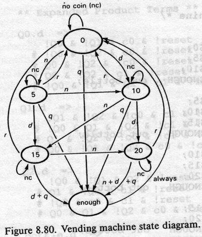
- We'll use the right-hand button to indicate nickel (i.e. you insert a 5-cent coin), then dime, then quarter.
- The left-hand button will reset the vending machine to its initial state, just in case
- I have provided the next-state logic for the reset and the nickel buttons.
- Your mission is to extend this logic to include the dime and quarter buttons as well.
- Here is my Verilog code: lab11e_part2.v
- Be sure to bug me with questions about anything that you don't understand!!
- Challenge: if you have extra time, add two more states called VEND1 (state 6) and VEND2 (state 7).
- The next state from ENOUGH should be VEND1 (unconditionally)
- The next state from VEND1 should be VEND2
- The next state from VEND2 should be GOT0
- Make the 8888 pattern and the LEDs go ON for the ENOUGH and the VEND2 states but make them do something boring for the VEND1 state, so that you get two flashes when a soda can is dispensed.
- Bigger challenge if you have lots of time, find a way to make a sequence of states after ENOUGH that blinks the LEDs in an even more interesting pattern, e.g. zooming from right to left like the Knight Rider car's front lights:
