User:Ashmanskas/p364/2012/lab11f
From LaPET electronics
< User:Ashmanskas | p364 | 2012
PHYS 364, fall 2012, lab 11f
- i.e. day six of Lab #11: Wednesday, Dec t
- Here is a link to the sort-of reading for Monday: fall 2010 lecture 10
- Here are some Verilog notes that I wrote up for the 2010 course. They will help you to understand some of the new Verilog constructs that you will see in today's programs that we have not used before
- Here is a link to Monday's lab: lab11e
- Please answer my survey questions while you are in class today. These only concern the course content and format, not whether or not you think I did a good job.
- Xilinx "user constraint file" from last time: basys2.ucf
- Today there is nothing to program, nothing to email me. But there is one opamp circuit to build in Part 2!
- And you should bug Bill and Jose with questions until you understand the details of the music-playing state machine!
Part 1
overview
- Neither part of this lab requires you to do any programming, but there are several parts of my program that I want you to try to follow.
- If you want to modify this program to do something slightly different, please feel free!
- Also please feel free to ask Bill or Jose for help implementing ideas that you have for modifying the program to do something that you find interesting.
- Here is the Verilog file for part 1: lab11f_part1.v
- To make things simpler, you can avoid compiling your own program by using this pre-compiled .bit file: lab11f_part1.bit
- The main goal of this lab is to understand how much more powerful a state machine becomes when it is combined with a memory that contains a list of tasks for it to carry out.
- In this case, the tasks that our state machine will carry out consist of playing out a sequence of musical notes.
ROM
- I have stored into a ROM (Read Only Memory) a sequence of musical notes to play.
- http://en.wikipedia.org/wiki/Read-only_memory
- The format of the ROM is 256 words, each of which is 16 bits wide.
- Thus, the ROM has 8 address bits and 16 data bits. (Do you see how that follows from the previous statement?)
- For each note to play, I use one 16-bit integer to store the desired duration (in milliseconds) of the note.
- I use a second 16-bit integer to store the desired half-period (in microseconds) of the note; this is how I choose to represent the pitch.
- So the 256 memory locations of the ROM can store a total of 128 notes to play.
- If you read through the lecture notes that I recommended reading for Monday's class, you saw that a ROM can be implemented in logic as a gigantic multiplexer. And you may remember from last week's reading (reading11.pdf) that the ternary operator ((condition) ? yesvalue : novalue) is equivalent to a logical multiplexer.
- Here is how the Xilinx software prefers for me to write the Verilog code for a ROM:
// 256x16 ROM, i.e. 256 storage locations, each of which is 16 bits wide;
// how exactly you get Verilog to infer a ROM, a RAM, etc. is somewhat
// idiomatic and depends on the FPGA vendor's software (e.g. Xilinx);
// this is one acceptable way to tell Xilinx that you want a ROM
module rom256x16 ( output [15:0] dataout,
                   input  [7:0]  address );
    wire [7:0] A = address;  // abbreviation to reduce typing
    // white piano keys starting from middle C:
    //    note:     C    D    E    F    G    A    B   C
    // f   (Hz):   262  294  330  349  392  440  494 523
    // T/2 (ms):  1911 1703 1517 1432 1276 1136 1012 956
    assign dataout =
      //    duration       halfperiod
      A==  0 ? 1000  :  A==  1 ? 1517  :
      A==  2 ? 1000  :  A==  3 ? 1703  :
      A==  4 ? 1000  :  A==  5 ? 1911  :
      A==  6 ? 1000  :  A==  7 ? 1703  :
      A==  8 ? 1000  :  A==  9 ? 1517  :
      A== 10 ? 1000  :  A== 11 ? 1517  :
      A== 12 ? 1000  :  A== 13 ? 1517  :
      A== 14 ? 1000  :  A== 15 ? 1703  :
      A== 16 ? 1000  :  A== 17 ? 1703  :
      A== 18 ? 1000  :  A== 19 ? 1703  :
      A== 20 ? 1000  :  A== 21 ? 1517  :
      A== 22 ? 1000  :  A== 23 ? 1276  :
      A== 24 ? 1500  :  A== 25 ? 1276  :
      A== 26 ? 1000  :  A== 27 ?    0  : // rest 1s
...
      A==250 ?    0  :  A==251 ?    0  :
      A==252 ?    0  :  A==253 ?    0  :
      A==254 ?    0  :  A==255 ?    0  : 0 ;
endmodule
- The input to the ROM is an 8-bit address. The output of the ROM is a 16-bit data value.
- In this ROM implementation, the expressions A==0, A==25, A==255, etc. represent the addresses; the expressions after the question marks represent the corresponding data values stored at those addresses.
- So this ROM stores the value 1703 at address 15, stores the value 1500 at address 24, etc.
- Remember that a 16-bit integer can hold a value from 0..65535.
- If you hold down Button #1 (2nd from right), you can set the ROM address to the 8-bit value set by the sliding switches, and the 16-bit ROM data at that address will display on the four digits of the 7-segment display.
- My state machine expects the ROM to be organized into pairs of 16-bit words. Locations 0, 2, 4, 6, 8, ... contain the durations (in milliseconds) of the notes to play, the locations 1, 3, 5, 7, 9, ... contain the pitch values (stored as half-period in microseconds).
- As a special case, if the half-period equals zero, I use that to indicate a "rest" (i.e. silence) instead of an audible note.
- As another special case, if the duration equals zero, then I use the corresponding half-period value to indicate the address from which the machine should subsequently start reading. This allows me to do a "GOTO" operation, so that, for example, at the end of a tune, I can go back and play the same tune again.
- Make sure that you understand the point of this "GOTO" operation before you finish going through Part 1, because it is a key idea that will help you on Friday to understand how a computer does its work.
- The idea is that I can store into the memory a value that is then used as a subsequent memory address.
state diagram
- Here is my state diagram for the machine that will read this ROM to play out a tune:
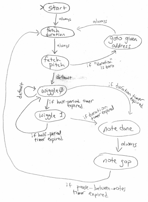
- Here is my list of states in Verilog:
    // Enumerate the possible states of our state machine
    localparam
      START=0,       // initial state: reset goes here
      FETCHDURA=1,   // fetch next note's duration (unit=millisecond)
      FETCHPITCH=2,  // fetch next note's half-period (unit=microsecond)
      GOTO=3,        // special case (duration==0): GOTO new memory address
      WIGGLE0=4,     // output bit is LOW for one-half period
      WIGGLE1=5,     // output bit is HIGH for one-half period
      NOTEDONE=6,    // finished playing a note
      NOTEGAP=7;     // pause briefly before moving on to next note
state representation in Verilog
- Since there are 8 states, I use a 3-bit-wide D-type flip-flop to hold the current state of the machine, which is called state. The logic to decide which state to enter on the next clock cycle will manipulate the wires called nextstate.
- By the way, this instantiation of a 3-bit flip-flop looks a bit different from before.
- To understand it in detail, look at my 2010 Verilog Notes.
- One thing that is different is that I have written a general-purpose N-bit flip-flop module, and when I instantiate it, I use (.N(3)) to indicate that the number of bits (N) should be 3 in this instance.
- Another thing that is different is that I am connecting the top-level wires to the module input/output wires by name instead of by position. So then I can write the inputs/outputs in whatever order I wish, and Verilog will not get confused about which top-level wires connect to which module inputs and outputs. It also makes it more clear to the person reading the program which argument is doing what.
- Here is the instantiation of the 3-bit-wide D-type flip-flop:
    // We'll use a 3-bit D-type flip-flop to hold the state of the FSM
    wire [2:0] state, nextstate;
    dffe_Nbit #(.N(3)) mystatedff
      (.q(state),        // on each rising edge of the clock, the flip-flop
       .d(nextstate),    //   copies 'nextstate' (D) to 'state' (Q)
       .clock(clock),    // clocked at 1 MHz
       .enable(1),       // always enabled
       .reset(reset));   // reset to initial state by pushing button
Next-state logic
- Here is the logic for the nextstate variable, which determines which state we will go into on the next clock cycle:
    // Compute next state based on current state and pertinent conditions
    assign nextstate =
      (reset || stopthenoise)             ? START      :  // go here if reset
      (state==START || forcenewaddress)   ? FETCHDURA  :
      (state==FETCHDURA)                  ? FETCHPITCH :
      (state==FETCHPITCH && zeroduration) ? GOTO       :  // dur==0 means GOTO
      (state==FETCHPITCH)                 ? WIGGLE0    :
      (state==GOTO)                       ? FETCHDURA  :
      (state==WIGGLE0 && durationup)      ? NOTEDONE   :  // end of this note?
      (state==WIGGLE0 && zeroperiod)      ? WIGGLE0    :  // rest vs. tone
      (state==WIGGLE0 && wigglenow)       ? WIGGLE1    :  // wiggle up & down
      (state==WIGGLE1 && durationup)      ? NOTEDONE   :
      (state==WIGGLE1 && wigglenow)       ? WIGGLE0    :
      (state==NOTEDONE)                   ? NOTEGAP    :
      (state==NOTEGAP && notegapdone)     ? FETCHDURA  :  // pause betw. notes
      /* default: stay in same state */     state      ;
- If we press the reset button (btn[0], the right-hand button), or if we slide the stopthenoise switch (sw[0], the right-hand switch) upward, then the machine goes to the START state. This is also where it starts when we first configure the FPGA.
- From the START state, the next state is always the FETCHDURA state.
- The FETCHDURA state goes to the next ROM address (which should be an even-numbered address) and records the 16-bit "duration" (in milliseconds) of the next note to play.
- We also go into the FETCHDURA state if the forcenewaddress button is pressed (which is btn[1], the second button from the right). This button allows the user (that's you) to directly modify the machine's address, so that the machine subsequently starts playing music from that address.
- From the FETCHDURA state, the next state is always the FETCHPITCH state.
- The FETCHPITCH state goes to the next ROM address (which should be an odd-numbered address) and records the 16-bit "halfperiod" (in microseconds) of the next note to play.
- From the FETCHPITCH state, there are two possible next states.
- By far the most common transition is to go to the WIGGLE0 state, which is used along with WIGGLE1 to make the output bit oscillate (wiggle) back and forth to make the desired musical tone.
- But in the special case in which the "duration" value is zero, we interpret this to mean that the "halfperiod" value actually represents the next memory address from which we should continue reading musical notes. In that case, the next state will be the GOTO state, to handle this change of address.
- If we happen to have wound up in the GOTO state, the next state from there is always the FETCHDURA state, from which the process begins of fetching from memory the next musical note to play.
- Again, the point of the GOTO state is to make the memory address jump discontinuously to a new location. Normally the memory address just increases one step at a time, incrementing once to find a new duration and then incrementing again to find a new pitch.
- We will look at the address-update logic in a moment.
- While a note is playing, we go back and forth between the WIGGLE0 state and the WIGGLE1 state.
- If we're in WIGGLE0, the output bit is LOW; if we're in WIGGLE1, the output bit is HIGH.
- We zero a microsecond counter before entering the WIGGLE0 or WIGGLE1 state. When the counter reaches the halfperiod value, we know it is time to transition to the other state, so that the output pin goes back and forth between LOW and HIGH at the correct oscillation period.
- Meanwhile, in the FETCHPITCH state, we zeroed a millisecond counter. If the number of milliseconds elapsed reaches the duration value, we know it is time to transition to the NOTEDONE state, to finish up playing this note and move on.
- There is one more special case: if halfperiod is zero, indicating that we should play silence (a rest) rather than a note, then we just stay in the WIGGLE0 state instead of going back and forth between WIGGLE0 and WIGGLE1.
- From the NOTEDONE state, we always go to the NOTEGAP state.
- The purpose of this state is to put a small (currently 25 milliseconds) gap between notes, so that your ear can hear the difference between two consecutive eighth-notes and a single quarter-note at the same pitch.
- I didn't realize that I needed this state until I heard how terrible Mary Had a Little Lamb sounded without it.
- If not otherwise specified, we just remain in the same state for the next clock cycle.
ROM address & instantiation
- The memory address from which to read is stored in an 8-bit D-type flip-flop.
- Notice that we again use the generalized dffe_Nbit with #(.N(8)) to indicate an 8-bit-wide flip-flop
    // Use an 8-bit D-type flip-flop to hold the memory address
    // from which the state machine is reading
    wire [7:0] memory_addr, memory_nextaddr;
    dffe_Nbit #(.N(8)) memaddrff
      (.q(memory_addr),
       .d(memory_nextaddr),
       .clock(clock),
       .enable(1), .reset(0));
- Next, we instantiate the ROM: it needs to know its address (input) and where to stick its data (output)
    // We will store the desired tune to be played in a ROM (Read-Only
    // Memory) with 256 locations, each of which can store a 16-bit number;
    // declare wires to store the 'dataout' value from the memory, as well
    // as the 'duration' and 'halfperiod' that will be copied (via flip-flops)
    // from the 'memory_data' wires
    wire [15:0] memory_data, duration, halfperiod;
    rom256x16 myrom1
      (.dataout(memory_data),   // data comes out
       .address(memory_addr));  // address goes in
- Here is the logic to decide what ROM address to read from on the next clock cycle:
    // Compute what memory address we will read from on next clock cycle
    assign memory_nextaddr =
      (btn[1])            ? sw[7:0]       :  // button1: goto switch address!
      (state==START)      ? 0             :  // start reading from zero
      (state==FETCHDURA)  ? memory_addr+1 :  // after reading duration or
      (state==FETCHPITCH) ? memory_addr+1 :  //   pitch, increment address
      (state==GOTO)       ? halfperiod    :  // special GOTO command
      /* default: same */   memory_addr   ;  // otherwise stay unchanged
- As a special case, if we hold down btn[1], the address is loaded from the sw[7:0] sliding switches.
- On the START state, we start out at address zero.
- If we are in either the FETCHDURA state or the FETCHPITCH state, we want to increment the address by one so that the next read will happen from the next memory location after this one.
- If we are in the GOTO state, then the halfperiod value (described below) contains the next address from which we should continue reading.
duration and halfperiod flip-flops
- We store the duration and the half-period for the current note in a pair of 16-bit flip-flops.
- The duration wires and the halfperiod wires connect the outputs of these flip-flops, respectively.
- The duration flip-flop is only enabled in the FETCHDURA state; and the halfperiod flip-flop is only enabled in the FETCHPITCH state.
- In both cases, the D (data) inputs of the flip-flops are from the memory_data outputs of the ROM. We're just writing down the value that we read from the ROM in either the FETCHDURA or the FETCHPITCH state.
- This is an important point. If you don't follow it, ask Bill or Jose!
    // Use a 16-bit D-type flip-flop to hold the desired duration (in ms)
    // the note we are playing (or are about to play)
    dffe_Nbit #(.N(16)) durationff
      (.q(duration),               // output goes to 'duration' wires
       .d(memory_data),            // input data come from memory output data
       .enable(state==FETCHDURA),  // enabled only in the FETCHDURA state
       .clock(clock), .reset(0));
    assign zeroduration = (duration==0);  // indicates special 'GOTO' command

    // Use a 16-bit D-type flip-flop to hold the half-period (in us)
    // of the note we are playing (or are about to play)
    dffe_Nbit #(.N(16)) halfperiodff
      (.q(halfperiod),              // output goes to 'halfperiod' wires
       .d(memory_data),             // input data come from memory output data
       .enable(state==FETCHPITCH),  // enabled only in the FETCHPITCH state
       .clock(clock), .reset(0));
    assign zeroperiod = (halfperiod==0);  // indicates rest (silence) vs. note
Counters for milliseconds and microseconds
- Now we have two 16-bit counters. One of them increments once per microsecond. (It does this easily because we chose our master clock to run at 1 MHz.)
- The second clock increments once per millisecond. But we still clock it with the same 1 MHz clock. We use a once-per-millisecond pulse called pulse_1kHz to enable the millisecond counter.
- We do this because we want all of the logic in our state machine to be synchronous to a single clock.
    // Use a 16-bit counter to count off microseconds until the next
    // time the wire driving the speaker needs to wiggle up or down
    wire [15:0] count_usec;
    wire        reset_usec;
    counter_Nbit #(.N(16)) myuseccounter
      (.q(count_usec),
       .clock(clock),        // clocked by 1 MHz clock
       .enable(1),           // always enabled
       .reset(reset_usec));  // reset to zero when starting new half-period
    // We start a new half-period immediately after FETCHPITCH or once
    // the number of microseconds exceeds the desired half-period
    assign reset_usec = (state==FETCHPITCH || wigglenow);
    assign wigglenow  = (count_usec==halfperiod);

    // Use a 16-bit counter to count off milliseconds until the end
    // of the note that we are playing (or are about to play)
    wire [15:0] count_msec;
    wire        reset_msec = (state==FETCHPITCH || state==NOTEDONE);
    counter_Nbit #(.N(16)) mymseccounter
      (.q(count_msec),       // elapsed millisecs (i.e. counter value)
       .clock(clock),        // counter operates from 1 MHz clock
       .enable(pulse_1kHz),  // enable only once per millisecond
       .reset(reset_msec));  // reset when starting or ending a note
    assign durationup = (count_msec==duration);
    assign notegapdone = (count_msec==25);  // 25 msec gap between notes
other connections
- Finally, notice that the left-hand pin on the JC connector is the wire that wiggles between LOW and HIGH when the state machine goes back and forth between the WIGGLE0 and WIGGLE1 states. You will want to connect this pin (the left-hand pin of JC) to one side of a small speaker. Connect the other side of the speaker to the GND wire (the 2nd pin from the right on the JC connector).
- Also notice that the LEDs display in binary what note we are currently playing (i.e. its half-period)
- If you hold down btn[1], then the 7-segment LEDs display the 16 bits of memory_data, so that you can see what is stored inside the ROM
- If you hold down btn[1], then the 8 bits of memory_address will be updated to contain whatever value is on the sliding switches, again so that you can inspect the ROM contents.
- If you are not holding down btn[1] (normally you won't be!), then the digits do this:
- Digit 0 indicates how much time is left until the current note is finished playing
- Digit 1 indicates what state the machine is in. It's a bit confusing that it appears to display a '9' much of the time, but this is really just going back and forth quickly between '4' and '5'.
- Digits 3 and 2 display the 8-bit memory_address from which the machine is currently reading.
    // Connect useful values to the inputs of 'myd4d1' (displaydigits module)
    wire [15:0] timeleft = duration-count_msec;
    assign digit0 = btn[1] ? memory_data[3:0]   : timeleft[14:7];
    assign digit1 = btn[1] ? memory_data[7:4]   : state;
    assign digit2 = btn[1] ? memory_data[11:8]  : memory_addr[3:0];
    assign digit3 = btn[1] ? memory_data[15:12] : memory_addr[7:4];
    assign dots[2:0] = btn[3:0];
    assign led = halfperiod[7:0];

    // Use 4 JC pins and 4 JD pins as outputs to drive LEDs, etc.
    assign jc[1] = (state==WIGGLE1);
    assign jc[4:2] = 0;
    assign jd[4:1] = {clock,pulse_1kHz,count_msec[0],count_msec[15]};
other tunes: the pips
- I assume that by now you have heard your board (and your neighbor's board) play a horrible rendition of Mary Had a Little Lamb over and over again. Yuck!
- You might at least want to go through the first several lines of the ROM contents and see how I managed to code in E, D, C, D, E, E, E, D, D, D, E, G, G, and so on.
- If you slide the switches to contain the decimal value 64 (binary 01000000) and momentarily hold down btn[1], then you will hear over and over again every ten seconds the pips that are played e.g. by the BBC World Service on the hour.
- See if you can understand how this is coded into the ROM:
      A== 64 ? 1000  :  A== 65 ?    0  : // BBC news GMT "pips"
      A== 66 ?  100  :  A== 67 ?  500  : // 1 kHz for 100 ms at :59:55
      A== 68 ?  900  :  A== 69 ?    0  :
      A== 70 ?  100  :  A== 71 ?  500  : // 1 kHz for 100 ms at :59:56
      A== 72 ?  900  :  A== 73 ?    0  :
      A== 74 ?  100  :  A== 75 ?  500  : // 1 kHz for 100 ms at :59:57
      A== 76 ?  900  :  A== 77 ?    0  :
      A== 78 ?  100  :  A== 79 ?  500  : // 1 kHz for 100 ms at :59:58
      A== 80 ?  900  :  A== 81 ?    0  :
      A== 82 ?  100  :  A== 83 ?  500  : // 1 kHz for 100 ms at :59:59
      A== 84 ?  900  :  A== 85 ?    0  :
      A== 86 ?  500  :  A== 87 ?  500  : // 1 kHz for 500 ms at :00:00
      A== 88 ? 4500  :  A== 89 ?    0  :
      A== 90 ?    0  :  A== 91 ?   64  : // goto address 64
- Do you understand now why I need a GOTO instruction so that after reading from addresses 90 and 91 the machine can be told to loop back to address 64?
other tunes: invention 13
- Here is a much more interesting tune. I actually transcribed the whole thing a couple of years ago, but there was a limit to what I could fit into the available memory.
- It starts at ROM address 96 (decimal), or 01100000 (binary).
- If you key this into the sw[7:0] and hold down btn[1] for a moment, it should start to play.
- By the way, if you get sick of the music at some point, you can slide sw[0] up and your machine should sit quietly in the START state.
Part 2
- I hope that after Part 1 (and after the previous two labs) you get the idea that a state machine is what allows a digital logic circuit to step through the kind of sequence of operations that you might normally ask a computer to carry out.
- The state machine from Part 1 was much more complicated than the vending-machine or traffic-signal state machines, though it does not really have such a huge number of distinct states.
- The main thing that makes this machine capable of doing something so complicated is that it is essentially reading a program from a memory and carrying out the instructions given in that memory.
- There is also no programming for this part (unless you feel like tinkering), but there is one opamp circuit to build.
- Here is the Verilog file for part 2: lab11f_part2.v
- To make things simpler, you can avoid compiling your own program by using this pre-compiled .bit file: lab11f_part2.bit
- The main point of this part is to remind you that a Verilog program is really not a program at all, but just a representation of a schematic diagram.
- I've taken the state machine from Part 1 and encapsulated it into a module called playerpiano, which you can look through in the Verilog source code.
- Then on the top level of the schematic diagram, I've instantiated two copies of playerpiano, reading from two separate ROMs and sending their output music to two separate FPGA pins: JC[1] (the left-hand pin on connector JC) and JD[1] (the left-hand pin on connector JD).
- If you load the program and plug your speaker from JC[1] to GND, you will hear the same tune as at the end of Part 1.
- If you move your speaker wire from JC[1] to JD[1], then you will hear the corresponding left-hand part of Invention 13.
- Notice that the two tunes are playing at the same time. The 7-segment display is showing the left-hand memory address with digits 3,2 and the right-hand memory address with digits 1,0.
- Here is your mission:
- Using one opamp and several resistors, wire up a circuit that allows you to combine the audio signals from the two FPGA output pins and send the combined (summed) signal to a single speaker.
- As an option, you might also contemplate a way to mix the two inputs with a ratio other than 1:1. Maybe you want the right-hand tune to be twice as loud as the left-hand tune, for instance.
- This should be a good way to refresh your memory of opamp circuits before the exam.
- Please try very hard not to expose the FPGA output pins to any voltage lower than 0 volts or higher than +3.3 volts, to avoid cooking the FPGA.
- In action: http://www.youtube.com/watch?v=_-ftw98K23w
- With bigger speaker and improved amplification: http://www.youtube.com/watch?v=tHcDawYmWtE
