User:Ashmanskas/p364/2012/lab11g
From LaPET electronics
< User:Ashmanskas | p364 | 2012
Contents |
PHYS 364, fall 2012, lab 11g
- i.e. day seven of Lab #11: Friday, Dec 7
- last day of class!
- Here is a link to the sort-of reading for Monday: fall 2010 lecture 10
- Here is a link to today's reading: reading11c.pdf
- Here are some Verilog notes that I wrote up for the 2010 course. They will help you to understand some of the new Verilog constructs that first appeared in Wednesday's programs that we had not used before then
- Here is a link to Wednesday's lab: lab11f
- Please answer my survey questions while you are in class today. These only concern the course content and format, not whether or not you think I did a good job. (The latter is something you tell the Registrar anonymously.)
- Xilinx "user constraint file" from last time: basys2.ucf
- Today there is nothing to program, nothing to email me.
- And you should bug Bill and Jose with questions until you understand the details of the CPU state machine!
Part 1
- If you didn't manage to get Wednesday's opamp circuit working to your satisfaction, feel free to spend the first half hour or so of today's lab session making that work. It's up to you whether or not you want to do this.
- If you got the opamp circuit to work but were unhappy with the sound quality (too quiet, too distorted), the most likely problem is the 25mA limit on the output current of the 741 opamp.
- Remember that the input resistance of the speaker is only about 8Ω, and the HIGH voltage of each FPGA pin is +3.3V. Depending on the resistor choices in your opamp circuit, you potentially have six volts or more from the opamp trying to drive the 8Ω speaker, i.e. well above the 25mA opamp limit.
- If you want to try to remove the distortion (but have a very quiet output), you can try putting a resistor in series with the speaker so that the current doesn't exceed the 25mA limit of the 741.
- Alternatively, try using a single NPN transistor (2N3904) and a single resistor (around 1KΩ should do) to make an emitter follower to follow the opamp circuit, to let you drive the speaker with a larger current. That should allow you to make quite a bit more noise.
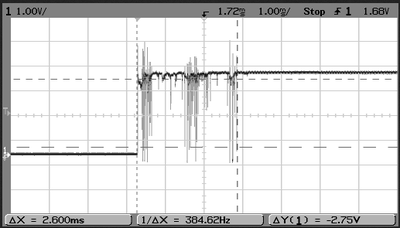
- Also, if you didn't have a chance on Wednesday to look at the musical waveforms using the oscilloscope, I highly recommend it.
- If you can get the fourier transform feature (in the "math" function selection) to work as well, so much the better. I saw it work on at least one scope on Wednesday, but some tinkering with the horizontal scale was necessary to get a clear peak to show up for each note.
Part 2
overview
- You don't need to do any Verilog programming today, but I want you to study and tinker with today's circuit enough that you can follow the key ideas.
- In part 3 you will modify the FPGA's memory contents to alter the program's behavior.
- In principle, you could load the FPGA with an entire instruction sequence of your own design, but that would require quite a bit of work — probably too much to fit into a lab session.
- If you want to modify my Verilog program to do something slightly different, absolutely feel free!
- Also please feel free to ask Bill or Jose for help implementing ideas that you have for modifying the program to do something that you find interesting.
- Here is the Verilog file: lab11g_part2.v
- If you decide to compile this file for yourself (though you don't need to), then you will also need to download asm.hex and stick it into the same ISE project directory that contains lab11g_part2.v
- You might as well keep reading through my description of each section of the Verilog code before you spend a lot of time staring at the whole lab11g_part2.v file.
- To make things simpler, you can avoid compiling your own program by using this pre-compiled .bit file: lab11g_part2.bit
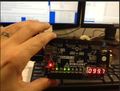
- If you use the ADEPT software to load this lab11g_part2.bit file into your BASYS2 board, you will see your board display a sequence of prime numbers. (Make sure the sliding switches are all in the DOWN positions.)
- The main goal of Wednesday's lab was to understand how much more powerful a state machine becomes when it is combined with a memory that contains a list of tasks for it to carry out. You saw on Wednesday that a state machine having a mere 8 states was able, when combined with a memory and a few counters, to act as a player piano.
- The main goal of today's lab is to go a step further, to see that the microprocessor at the heart of your Arduino, iPhone, desktop computer, etc. is really just a fancy state machine connected to a large memory.
state diagram
- Hopefully this state diagram looks reasonably familiar from the reading (file reading11c.pdf online):
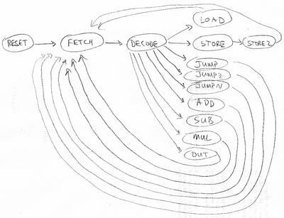
- This is basically the same state diagram that appeared in the reading, except that I created additional opcodes for JUMPZ (jump if AC==0), JUMPN (jump if AC<0), SUB (subtract memory contents from accumulator), MUL (multiply accumulator by memory contents), and OUT (display accumulator on 7-segment LED display).
- Here is what this list of states looks like in Verilog:
    // Enumerate the possible states of CPU's state machine
    localparam
      RESET  =  0,  // initial state: reset goes here
      FETCH  =  1,  // fetch next instruction from memory
      DECODE =  2,  // decode instruction: what are my orders?!
      LOAD   =  3,  // execute LOAD:   AC := memory[argument]
      STORE  =  4,  // execute STORE:  memory[argument] := AC
      STORE2 =  5,  //   store gets an extra clock cycle for write to finish
      JUMP   =  6,  // execute JUMP:   PC := argument
      JUMPZ  =  7,  // execute JUMPZ:  if (AC==0) PC := argument
      JUMPN  =  8,  // execute JUMPN:  if (AC<0) PC := argument
      ADD    =  9,  // execute ADD:    AC := AC + memory[argument]
      SUB    = 10,  // execute SUB:    AC := AC - memory[argument]
      MUL    = 11,  // execute MUL:    AC := AC * memory[argument]
      OUT    = 12;  // execute OUT:    display AC on 7-segment LEDs
- Since there are 13 states (somewhat less than 16), I use a 4-bit-wide D-type flip-flop to hold the current value of the CPU state:
    // Use a 4-bit D-type flip-flop to hold the state of the CPU's FSM
    dffe_Nbit #(.N(4))  state_ff (.q(state), .d(state_next),
				  .clock(clock), .enable(run), .reset(reset));
- and here is the next-state logic to set up the transitions from state to state:
    // Compute next state based on current state and pertinent conditions
    assign state_next =
      reset         ? RESET                 :  // reset line => RESET
      state==FETCH  ? DECODE                :  // FETCH => DECODE
      state==DECODE ? (IR[15:8]==0 ? LOAD   :  // DECODE => execute decoded
                       IR[15:8]==1 ? STORE  :  //   instruction (LOAD, STORE,
                       IR[15:8]==2 ? JUMP   :  //   JUMP, etc.)
                       IR[15:8]==3 ? JUMPZ  :
                       IR[15:8]==4 ? JUMPN  :
                       IR[15:8]==5 ? ADD    :
                       IR[15:8]==6 ? SUB    :
                       IR[15:8]==7 ? MUL    :
                       IR[15:8]==8 ? OUT    :
                                     FETCH) :  // unknown => FETCH
      state==STORE ? STORE2                 :  // STORE => STORE2
      /* default */  FETCH                  ;  // default => FETCH
- As the reading described, the CPU points its "Program Counter" at the next address in memory, FETCHes the instruction from memory[PC], and then DECODEs it to figure out what to do next.
- The upper 8 bits of the instruction contain the "opcode," i.e. they determine whether the instruction is a LOAD operation, a STORE operation, an ADD operation, etc.
- The lower 8 bits of the instruction are the "argument" for the operation, and generally refer to a memory address.
Random Access Memory
- This CPU uses a read/write memory, a.k.a. a Random Access Memory (RAM) both to store the instructions that it will execute and to store the intermediate results of its calculations.
- The module that defines the RAM begins like this:
// 256x16 RAM, i.e. 256 storage locations, each of which is 16 bits wide
module ram256x16 (
    input         clock,        // clock (pertinent for writes only)
    input         writeenable,  // write-enable
    input  [7:0]  address,      // address at which to read/write
    input  [15:0] datain,       // data to store next clock (if write-enabled)
    output [15:0] dataout       // current memory contents at address A
);
- The other details of this ram256x16 module are not worth studying, except to note that the initial ("power-up") contents of the memory, when the FPGA is first configured by the ADEPT software, are read from a file called asm.hex
- It turns out that I could have used this convenient hexadecimal file format for the music-machine's memory, but I didn't figure out until yesterday how to make this file format work with the Xilinx software.
- I will show you down below how to make sense of the data stored in the RAM.
- To connect this memory to our CPU state machine, we need to connect the 8-bit memory_addr lines, the 16-bit memory_datain lines, the single memory_write line (which is HIGH only when we want to update the value stored in the memory at the current address), and the 16-bit memory_dataout lines. The first three of these are outputs of the CPU state machine (they are inputs to the memory), so they are connected like this:
    // This CPU uses a RAM consisting of 256 16-bit words.  In the
    // FETCH state, the memory address is the Program Counter, so that
    // we can fetch the next instruction.  Otherwise, the memory
    // address is the "argument" of the decoded instruction, i.e. the
    // low 8 bits of the IR.
    assign memory_addr = (state==FETCH) ? PC : IR[7:0];

    // The memory is only written in the STORE state; the data written
    // to the memory always come from the accumulator (AC).
    assign memory_write  = (state==STORE);
    assign memory_datain = AC;
- The memory_dataout lines are an input to the CPU (they are an output of the memory); we will see below how they are used.
Accumulator
- The accumulator is the register that does nearly all of the CPU's work. It is stored in a 16-bit-wide D-type flip-flop. Here is the Verilog code that instantiates the flip-flop and connects it:
     // Accumulator (AC) is this CPU's primary register; all math
     // instructions operate on the accumulator.
     //
     // Acccumulator next-value logic:
     //   ADD    =>  AC := AC + memory
     //   SUB    =>  AC := AC - memory
     //   MUL    =>  AC := AC * memory
     //   LOAD   =>  AC := memory
     //   RESET  =>  AC := 0
     //
     // Note that the multiply happens in a single clock cycle, so it
     // will compile to an entirely combinational multiplier -- the
     // one you would write down using an adder and a multiplexer for
     // each bit of the multiplicand.
    dffe_Nbit #(.N(16)) AC_ff (.q(AC), .d(AC_next), .clock(clock),
                               .enable(AC_enable), .reset(reset));
    assign AC_next  = (state==ADD)  ? AC + memory_dataout :
                      (state==SUB)  ? AC - memory_dataout :
                      (state==MUL)  ? AC * memory_dataout :
                      (state==LOAD) ? memory_dataout      : 0;
    assign AC_enable =  run &&
			(state==ADD  ||
			 state==SUB  ||
			 state==MUL  ||
			 state==LOAD ||
			 state==RESET );
- It is actually really neat (I think) to see how the contents of the accumulator are transformed when the CPU is in the various states like LOAD, ADD, SUB, MUL.
output register
- The output register is how this little CPU communicates its results to the outside world.
- When the OUT instruction is executed, the current contents of the accumulator are copied to the OUT register, whose contents are always displayed on the 4-digit 7-segment LED display.
- On a real computer, a mechanism similar to this would be used to interface the computer to a digital-to-analog converter, or to external devices like printers, network interfaces, disk drives, etc.; a real computer would also have an opcode like IN to receive input from external devices like keyboards, mice, analog-to-digital converters, disk drives, etc.
- Here is the Verilog code for the output register:
    // The output register is this CPU's way to report its results to
    // the outside world.  The only path to the 'out' register is from
    // the accumulator.  The 'out' register is only enabled while the
    // OUT instruction is executing.
    dffe_Nbit #(.N(16)) out_ff (.q(out), .d(AC), .clock(clock),
                                .enable(out_enable), .reset(reset));
    assign out_enable = (state==OUT) && run;
Instruction Register
- The Instruction Register (IR) holds the 16-bit instruction that is currently being executed, as described in today's reading.
- Here is the Verilog code for the IR:
    // The Instruction Register (IR) holds the instruction that is
    // currently being executed.  The only path into the IR is from
    // the memory; the IR is only enabled in the FETCH state, i.e.
    // while fetching the next instruction from memory.
    dffe_Nbit #(.N(16)) IR_ff (.q(IR), .d(memory_dataout), .clock(clock),
                               .enable(IR_enable), .reset(reset));
    assign IR_enable = (state==FETCH) && run;
Program Counter
- The Program Counter (PC) holds the memory address from which the next instruction will be read, the next time the CPU enters the FETCH state.
- Normally the Program Counter just increases by one on each subsequent instruction, corresponding to running a program that has no GOTOs, no loops, etc.
- But the JUMP, JUMPZ, and JUMPN opcodes can overwrite the contents of the Program Counter, thus changing the flow of the program.
- The conditional jump instructions are the most interesting ones, as they are what permit the computer to make decisions: it can e.g. (JUMPZ instruction) go to a different address if the accumulator currently equals zero, or else continue along its current path if the accumulator contents are non-zero
- Similarly, we can check whether the accumulator is negative (i.e. the highest bit is set), and jump or not jump accordingly.
- It turns out that if you want to figure out whether B is greater than A, you subtract B from A and then see whether or not the result is negative. That is the usual way that computers make comparisons of two numbers. Isn't that clever of them?
- You can also figure out of B equals A by subtracting B from A and then testing to see whether the result is zero.
- Here is the Verilog code for the Program Counter:
    // The Program Counter (PC) holds the address from which the next
    // instruction will be fetched.  Here is the program counter
    // update logic:
    //    RESET    =>  PC := 0
    //    FETCH    =>  PC := PC+1  (after fetching from PC, point to PC+1)
    //    JUMP     =>  PC := low byte of IR
    //    JUMPZ    =>  PC := low byte of IR if AC == 0, else unchanged
    //    JUMPN    =>  PC := low byte of IR if AC <  0, else unchanged
    dffe_Nbit #(.N(8)) PC_ff (.q(PC), .d(PC_next), .clock(clock),
                              .enable(PC_enable && run), .reset(reset));
    assign PC_next  = (state==RESET) ? 0 :
                      (state==FETCH) ? PC+1 : IR[7:0] ;
    assign PC_enable = run &&
		       ((state==RESET)           ||
			(state==FETCH)           ||
			(state==JUMP)            ||
			(state==JUMPZ && AC==0)  ||
			(state==JUMPN && AC[15]));
top-level connections
- That's basically all it takes to make a simplified computer. You can see that it's just a state machine connected to a memory, not so different from Wednesday's music machine.
- I put the guts of the computer (a.k.a. CPU, Central Processing Unit) into a module called simple_cpu.
- Here are the connections needed from the top-level module:
    // These wires connect to the inputs/outputs of the CPU module
    wire [15:0] memory_dataout, memory_datain, IR, AC, out;
    wire [7:0]  PC, memory_addr;
    wire [3:0]  state;
    wire        memory_write;

    // Determine when the CPU will run (do its normal thing) and when
    // it will pause to wait for the user.
    wire run = !sw[0];

    // Button 1 will reset the CPU to its initial state.
    // function
    wire reset = btn[1];

    // Instantiate the CPU and its memory
    simple_cpu cpu (.clock(clock), .reset(reset), .run(run),
                    .PC(PC), .AC(AC), .IR(IR), .state(state),
                    .memory_dataout(memory_dataout), .memory_addr(memory_addr),
                    .memory_datain(memory_datain), .memory_write(memory_write),
                    .out(out));
    ram256x16 ram (.clock(clock),
		   .writeenable(memory_write),
                   .address(memory_addr),
		   .datain(memory_datain),
		   .dataout(memory_dataout));

    // The green LEDs will display the Program Counter
    assign led = PC;

    // The 7-segment display will show the OUT register, i.e. the most
    // recent prime number.
    wire [15:0] leddat = out;
....
    assign {digit3,digit2,digit1,digit0} = leddat;
- Everything else in the top-level module (lab11g) is stuff that has been there since Monday's or Wednesday's lab: the counter to make a 1 MHz clock from the on-board 50 MHz clock; the display4digits module and its connections, to handle the ping-pong updating of the 4 separate digits of the 7-segment display.
- You can see that there's not much to it.
- By the way, this little computer finds prime numbers about 50 times as fast if you use 'mclk' instead of 'clock' to clock the CPU. But around 8pm last night I realized that I had created an insidious bug by using 'mclk' for some of the logic and 'clock' for other logic. In the interest of time, I switched everything back to 'clock'.
Now what can it do?
- To prove to you that this computer is capable of doing a real computation, I coded the stupidest imaginable algorithm for calculating all of the prime numbers from 2 to 9973.
- Here is the algorithm if I were to write it in the C programming language:
- Stare at it for long enough to convince yourself that it can indeed identify prime numbers.
#include <stdio.h>

int main(void)
{
  int i, j, k, product;
  // loop 'i' over candidate prime numbers, from 2 to 9999
  for (i = 2; i<10000; i = i+1) {
    // loop 'j' over possible first factors, from 2 to i-1
    for (j = 2; j<i; j = j+1) {
      // loop 'k' over possible second factors, from j to i-1
      for (k = j; k<i; k = k+1) {
	product = j*k;
	// if j*k equals i, then i must not be prime: jump to 'iloop'
	if (product==i) goto iloop;
	// if j*k > i, then skip the rest of the k loop
	if (product>i) break;
      }
    }
    // if we reach this point, then i is prime: print it out
    printf("%d\n", i);
  iloop:;  // this label 'iloop' allows the 'goto' to jump here
  }
  return 0;
}
- When I run the above program on my Mac, I see this output (boring parts suppressed):
2
3
5
7
11
13
17
19
23
29
....
9887
9901
9907
9923
9929
9931
9941
9949
9967
9973
- Regrettably, I do not have a C compiler for our home-made computer. I have to write my program directly in the computer's assembly language, i.e. using the opcodes LOAD, STORE, ADD, JUMP, etc.
- Here I go:
- Note that everything to the right of a '#' symbol is a comment.
        #
        # prime.sasm
        # coded 2010-11-11 by Bill Ashmanskas, ashmansk@hep.upenn.edu
        #
        # The purpose of this program is to demonstrate that the CPU
        # implemented in simple_cpu.v is capable of carrying out a
        # non-trivial computation.
        #
        # This is probably the dumbest imaginable algorithm to compute
        # prime numbers.  Its execution time scales as the third power
        # of the number of candidates to evaluate.  For every candidate i,
        # loop over possible factors j and k, testing whether i==j*k.  If
        # no such j and k are found, then display i on the LEDs.
        #
        # Note that with storage for a mere 5000 boolean values (which
        # I could have easily cooked up), one can use a much more efficient
        # algorithm, the Sieve of Eratosthenes.  It scales (with number of
        # candidate integers N) as N*log(N)*log(log(N)), while my algorithm
        # scales as N**3.  I point this out only so that you don't think
        # that I think the N**3 algorithm is a good way to compute primes.
        #
start:  load    istart  #
        store   i       #  i := istart (nominally 1)
iloop:  load    i       #  loop i from istart+1 to 9999
        add     one     #
        store   i       #    i := i+1
        load    d9999   #
        sub     i       #
        jumpn   done    #    if (i>9999) goto done
        load    one     #
        store   j       #    j := 1
jloop:  load    j       #    loop j from 2 to i-1
        add     one     #
        store   j       #      j := j+1
        load    i       #
        sub     j       #
        jumpz   jdone   #      if (j==i) goto jdone
        load    j       #
        sub     one     #
        store   k       #      k := j-1
kloop:  load    k       #      loop k from j to i-1
        add     one     #
        store   k       #        k := k+1
        sub     i       #
        jumpz   jloop   #        if (k==i) goto jloop
        load    j       #
        mul     k       #
        store   prod    #        product := j*k
        sub     i       #        // if j*k==i then i is not prime
        jumpz   iloop   #        if (product==i) goto iloop  // skip to next i
        jumpn   kloop   #        if (product<i)  goto kloop  // keep looping k
                        #        // k exceeds i/j, so skip to next j
        jump    jloop   #        goto jloop
        #
        # If we reach here, then i is a prime number.  The only purpose
        # of the code below is to convert i from binary into decimal so
        # that the LED display can be understood by human observers.
        #
jdone:  load    zero    #  'outnum' will hold the binary-coded decimal result
        store   outnum  #  outnum := 0

... (uninteresting stuff suppressed) ...

done:   jump    start   #  go back and start counting again from i==2
disply: load    outnum  #  send most recent prime to the 7-segment display
	out		#
        jump    iloop   #  go back up to try next candidate i
zero:   .data   0       #  store the constant '0'
one:    .data   1       #  store the constant '1'
i:      .data   0       #  store the loop variable 'i' (prime number cand.)
j:      .data   0       #  store the loop variable 'j'
k:      .data   0       #  store the loop variable 'k'
l:      .data   0       #  store the loop variable 'l'
prod:   .data   0       #  store the product 'prod' = j*k
outnum: .data   0       #  compute/store binary-coded-decimal conversion of i
remain: .data   0       #  store remainder used in BCD computation
hdigit: .data   0       #  store hex value used to display one decimal digit
h1000:  .data   1000    #  store hexadecimal constant 0x1000
h100:   .data   100     #  store hexadecimal constant 0x100
h10:    .data   10      #  store hexadecimal constant 0x10
d10000: .data   2710    #  store decimal constant 10000
d1000:  .data   3e8     #  store decimal constant 1000
d100:   .data   64      #  store decimal constant 100
d10:    .data   a       #  store decimal constant 10
d9999:  .data   270f    #  store decimal constant 9999 (= 270f in hexadecimal)
istart: .data   1       #  starting value for i (i.e. first prime to check)
Ndelay: .data   f000    #  delay factor (in hexadecimal)
- The part of the code that is shown above does the prime number calculation.
- The whole program, including parts that I omitted above, is at prime.sasm
- There are two parts that I didn't show:
- The conversion of the prime number from a 16-bit hexadecimal integer into four decimal digits (thousands, hundreds, tens, ones); if I didn't do this, then the prime numbers would print out in hexadecimal, which would make the program seem less convincing to a human observer.
- The brief delay before displaying each new prime number, so that the numbers do not overwrite each other too quickly for you to see.
- The delay is implemented simply as a loop: tell the computer to count to about 60000 as a way to waste time.
machine-readable format
- The program above is still in human-readable form. We need to convert the instructions into hexadecimal memory contents.
- Here is the output of that process, i.e. an annotated file that is identical in content to asm.hex
- The file looks like this (with boring parts suppressed):
        mem['h00] = 'h006b;  //  start:   load  istart
        mem['h01] = 'h015b;  //           store i
        mem['h02] = 'h005b;  //  iloop:   load  i
        mem['h03] = 'h055a;  //           add   one
        mem['h04] = 'h015b;  //           store i
        mem['h05] = 'h006a;  //           load  d9999
        mem['h06] = 'h065b;  //           sub   i
        mem['h07] = 'h0455;  //           jumpn done
        mem['h08] = 'h005a;  //           load  one
        mem['h09] = 'h015c;  //           store j
        mem['h0a] = 'h005c;  //  jloop:   load  j
        mem['h0b] = 'h055a;  //           add   one
        mem['h0c] = 'h015c;  //           store j
        mem['h0d] = 'h005b;  //           load  i
        mem['h0e] = 'h065c;  //           sub   j
        mem['h0f] = 'h031f;  //           jumpz jdone
        mem['h10] = 'h005c;  //           load  j
        mem['h11] = 'h065a;  //           sub   one
        mem['h12] = 'h015d;  //           store k
        mem['h13] = 'h005d;  //  kloop:   load  k
        mem['h14] = 'h055a;  //           add   one
        mem['h15] = 'h015d;  //           store k
        mem['h16] = 'h065b;  //           sub   i
        mem['h17] = 'h030a;  //           jumpz jloop
        mem['h18] = 'h005c;  //           load  j
        mem['h19] = 'h075d;  //           mul   k
        mem['h1a] = 'h015f;  //           store prod
        mem['h1b] = 'h065b;  //           sub   i
        mem['h1c] = 'h0302;  //           jumpz iloop
        mem['h1d] = 'h0413;  //           jumpn kloop
        mem['h1e] = 'h020a;  //           jump  jloop
        mem['h1f] = 'h0059;  //  jdone:   load  zero
        mem['h20] = 'h0160;  //           store outnum
...
        mem['h55] = 'h0200;  //  done:    jump  start
        mem['h56] = 'h0060;  //  disply:  load  outnum
        mem['h57] = 'h0800;  //           out
        mem['h58] = 'h0202;  //           jump  iloop
        mem['h59] = 'h0000;  //  zero:    .data 0
        mem['h5a] = 'h0001;  //  one:     .data 1
        mem['h5b] = 'h0000;  //  i:       .data 0
        mem['h5c] = 'h0000;  //  j:       .data 0
        mem['h5d] = 'h0000;  //  k:       .data 0
        mem['h5e] = 'h0000;  //  l:       .data 0
        mem['h5f] = 'h0000;  //  prod:    .data 0
        mem['h60] = 'h0000;  //  outnum:  .data 0
        mem['h61] = 'h0000;  //  remain:  .data 0
        mem['h62] = 'h0000;  //  hdigit:  .data 0
        mem['h63] = 'h1000;  //  h1000:   .data 1000
        mem['h64] = 'h0100;  //  h100:    .data 100
        mem['h65] = 'h0010;  //  h10:     .data 10
        mem['h66] = 'h2710;  //  d10000:  .data 2710
        mem['h67] = 'h03e8;  //  d1000:   .data 3e8
        mem['h68] = 'h0064;  //  d100:    .data 64
        mem['h69] = 'h000a;  //  d10:     .data a
        mem['h6a] = 'h270f;  //  d9999:   .data 270f
        mem['h6b] = 'h0001;  //  istart:  .data 1
        mem['h6c] = 'hf000;  //  Ndelay:  .data f000
        mem['h6d] = 'h0000;
        mem['h6e] = 'h0000;
        mem['h6f] = 'h0000;
        mem['h70] = 'h0000;
...
- So the memory contents that cause the computer to calculate this big sequence of prime numbers look like this:
- 006b 015b 005b 055a 015b 006a 065b 0455 005a 015c 005c 055a 015c 005b 065c 031f 005c 065a 015d 005d 055a 015d 065b 030a 005c 075d 015f 065b 0302 0413 020a 0059 0160 005b 0161 0666 0426 0255 0059 0162 0061 0667 0430 0161 0062 0563 0162 0228 0062 0560 0160 0059 0162 0061 0668 043d 0161 0062 0564 0162 0235 0062 0560 0160 0059 0162 0061 0669 044a 0161 0062 0565 0162 0242 0062 0560 0561 0160 006c 015e 005e 065a 015e 0356 0250 0200 0060 0800 0202 0000 0001 0000 0000 0000 0000 0000 0000 0000 0000 1000 0100 0010 2710 03e8 0064 000a 270f 0001 f000 0000 0000 ... (more zeros)
- There's not much to it! It's shorter than yesterday's musical score.
- In the unlikely event that you're dying to know how I managed to convert the first format into the second format, here is the python program that I wrote to do the conversion: sasm.py
- Such a program is called an assembler, because it converts human-readable assembly language into hexadecimal (or binary) machine code
Part 3
- So far I haven't given you too much to do on your own.
- To make the little computer capable of being studied and prodded in action, I have added a bunch of additional logic to the top-level module that instantiates the simple_cpu module.
- It is not necessary for you to understand this additional logic, because its purpose is just to make it possible for you to tinker with the computer.
- But if you look through it, you probably won't find it too difficult to follow.
- The enhanced Verilog file is lab11g_part3.v
- The corresponding .bit file is lab11g_part3.bit
New features
- Reset button
- Actually this feature was there in Part 2, but we didn't use it. If you push btn[1] down, you will reset the CPU to its initial state, and it will re-start counting from 0002
- Pause switch
- This feature was also there in Part 2, though we didn't use it. If you slide sw[0] up, you will pause the CPU's activity.
- Program Counter display
- This feature was also there in Part 2. The 8 green LEDs display the current value of the Program Counter.
- New functions for 7-segment LEDs
- Finally, a new feature!
- If you slide sw[7] up, then the left two digits will display the Program Counter, and the right two digits will display the memory_addr, i.e. the address that is currently sent into the RAM.
- If you slide sw[6] up (but not sw[7]), then the four digits will display the Instruction Register.
- If you slide sw[5] up (but not sw[7:6]), then the four digits will display memory_dataout, i.e. the data that are currently read out of the RAM.
- If you slide sw[4] up (but not sw[7:5]), then the four digits will display the Accumulator contents.
- If you slide sw[3] up (but not sw[7:4]), then the right-hand digit will display the state number of the CPU's finite state machine, i.e. 0=RESET, 1=FETCH, 2=DECODE, etc.
- If you press btn[3], it will rotate between four modes of operation for the CPU.
- The decimal-point dots will display ---*, --*-, -*--, *--- respectively for modes 0, 1, 2, 3.
- In mode 0, the CPU runs freely as it did in Part 2. You can use sw[0] to pause the CPU and btn[1] to reset it.
- In mode 1, the CPU will pause at each OUT instruction until you press btn[0] to continue. This results in each prime number being displayed until you push btn[0]. While the CPU is stopped, you can use sw[7] through sw[3] to explore the contents of 7={PC,memaddr}, 6=IR, 5=memdataout, 4=AC, 3=state.
- In mode 2, the CPU will pause at each DECODE state until you press btn[0]. You can single-step through individual instructions and examine the CPU's registers using sw[7] through sw[3] as above.
- Also in mode 2, if sw[0] is HIGH, then the CPU will pause on every clock cycle, no matter what state it is in. You can watch the CPU's finite state machine go from FETCH to DECODE to (LOAD,STORE,ADD,etc.).
- In mode 0, 1, or 2, pressing btn[2] will copy the current 8-bit value represented by the sliding switches into a register called useraddr. When you are in mode 1 (not mode 2, this is mode 1 again), if the Program Counter equals the 8-bit value in useraddr, then the CPU will pause until you press btn[0]. This allows you to explore what the CPU is doing at a particular section of the program code. (If you are a programmer, it is like setting a breakpoint in the debugger.)
- So you can use the useraddr feature in mode 1 to make the program stop next time it reaches e.g. the instruction at address 18 (hexadecimal), then switch to mode 2 to single-step through the subsequent instructions.
- In mode 3, the CPU does nothing, and you have read/write access to the memory.
- If all of the sliding switches are LOW, then btn[0] will step forward through the memory one address at a time.
- In memory mode (mode 3), the 8 green LEDs show the address, and the digits show the memory data stored at that address.
- While you are holding down btn[0], the digits will momentarily show the address also.
- If the switches are set to a non-zero position, then pressing btn[0] will use the switches as the address into the memory. This address is remembered once the button is released, so you can then move the switches without changing the address.
- If you push btn[1], the 8-bit value from the switches will replace the lower 8 bits of the memory contents at the current memory address.
- If you push btn[2], the 8-bit value from the switches will replace the upper 8 bits of the memory contents at the current memory address.
- The "current memory address" in memory mode (mode 3) is stored in the same 'useraddr' register mentioned above.
- This allows you to look through the memory contents, compare it with the assembler output, and even modify the program (or more likely the .data words)
Your challenge
- See if you can change the contents of a single memory location to remove (or greatly reduce) the deliberate pause (currently about half a second) between successive prime numbers.
- You need to go into memory mode (mode 3), then find the address where the constant Ndelay is stored, then change it to a small number, like 1. (Why does changing it to 0 not work? Notice that the first thing the delay loop does is subtract one from the value it loads from Ndelay.)
- See if you can change the contents of a single memory location to make the computer just enumerate the prime numbers <= 100, then start over again, instead of finding every prime number <= 9999.
- You might want to change Ndelay back to a larger value before you do this, or else run the program in "mode 1" so that you can see each prime number appear.
- Now if you undo that last change, see if you can change the contents of a single memory location to make the computer start counting prime numbers from a much larger starting point, like 1000.
- Depending on how you interpret my suggestion of "1000," you may or may not be very surprised by the first number that emerges from the CPU.
- Notice that the program gets a lot slower as the prime numbers get larger. That is a result of the stupidity of this algorithm. Finding the primes up to 2000 takes it something like 8 times as long as finding the primes up to 1000 (if you let the program run at full speed), because it is using a triply-nested loop to do its computations.
- There is actually a much better algorithm for finding prime numbers: http://en.wikipedia.org/wiki/Sieve_of_Eratosthenes
- But I wanted to show you an algorithm that could be easily coded for this tiny computer.
- Let the program run for a while, and then see if you can find the memory location where the most recently computed prime number is stored. (If you pause the program somewhere in the delay loop, you will probably see the value that it has not yet written out to the display.) Also see if you can find where the current candidate hypothetical prime number 'i' is stored. Depending on where you pause the program, it should be the same as or a bit larger than the most recent prime that was displayed. You'll need to convert between hexadecimal and decimal to compare with the decimal value that is displayed while the program runs normally.
- Try modifying the instruction stored at address 08 (nominally 005a = "load one") so that instead it jumps unconditionally to label "jdone". The result should be that the program displays EVERY number, not just prime numbers.
- I just tried it — it works!
- This should continue to work if you use btn[1] to reset the CPU: it should start counting 2, 3, 4, 5, 6, 7, 8, 9, .... in decimal!
- If you then re-do the very first change, you should be counting very fast in decimal, up to 9999.
switch debouncer
- If you're curious about the debounce module that appears in lab11g_part3.v, you might want to learn about why mechanical switches need to be "debounced."
News flash! Bug fix!!
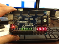
- Many thanks to Brian, Paul, and Thomas for pointing out the bug in my program that caused the prime number calculator to fail to identify 997, 1009, 1013, 1019, and 1021, for example.
- Here is the problem: when we consider possible factors of 997, our algorithm is naive enough to consider even rather large candidate factors, like 133*933, 271*971, or 331*399. For example, 331*399 = 132069. But our accumulator is only 16 bits wide, so the result of the 16-bit × 16-bit multiplication is 132069 & 0xffff, i.e. is truncated to 16 bits, giving what appears to be 997. Hah!
- There are two ways around this: a "software" fix, and a "hardware" fix.
- Here is the software fix:
- The idea is that we check whether j*j>i, and if so, we break out of the loop over j values, so effectively we loop j only up to sqrt(i).
start:  load    istart  #
        store   i       #  i := istart (nominally 1)
iloop:  load    i       #  loop i from istart+1 to 9999
        add     one     #
        store   i       #    i := i+1
        load    d9999   #
        sub     i       #
        jumpn   done    #    if (i>9999) goto done
        load    one     #
        store   j       #    j := 1
jloop:  load    j       #    loop j from 2 to i-1
        add     one     #
        store   j       #      j := j+1
        load    i       #
        sub     j       #
        jumpz   jdone   #      if (j==i) goto jdone
	load    j	## = ADD THIS CHECK TO PREVENT OVERFLOW IN MULTIPLY =
        mul     j	##
        sub     i	##
	jumpz	iloop	##     if (j*j==i) goto iloop  // perfect square
        jumpn   jok	##     if (j*j<i) goto jok
        jump    jdone	##     goto jdone
jok:    load    j	## = ============================================== =
        sub     one     #
        store   k       #      k := j-1
kloop:  load    k       #      loop k from j to i-1
        add     one     #
        store   k       #        k := k+1
        sub     i       #
        jumpz   jloop   #        if (k==i) goto jloop
        load    j       #
        mul     k       #
        store   prod    #        product := j*k
        sub     i       #        // if j*k==i then i is not prime
        jumpz   iloop   #        if (product==i) goto iloop  // skip to next i
        jumpn   kloop   #        if (product<i)  goto kloop  // keep looping k
                        #        // k exceeds i/j, so skip to next j
        jump    jloop   #        goto jloop
        #
        # If we reach here, then i is a prime number.  The only purpose
        # of the code below is to convert i from binary into decimal so
        # that the LED display can be understood by human observers.
        #
- Here is the complete assembly language source file: prime_uptosqrt.sasm
- Here is the assembler output: prime_uptosqrt_assembled.txt
- Here is the hexadecimal memory file: asm_uptosqrt.hex
- (This would need to be named 'asm.hex' to be found by the Xilinx compiler.)
- Here is the .bit file from Xiilnx ISE: lab11g_uptosqrt.bit
- Here is a YouTube video proving that the updated program now correctly finds 997, 1009, 1013, etc.:
- https://www.youtube.com/watch?v=g4wzzsKy2uo
- But note that this video reveals another software bug (!) which allows perfect squares to be declared prime. Oops. That bug is fixed in the source code shown above, but I didn't bother to re-make the YouTube video. You'll see in the video that 31*31=961 is incorrectly declared to be prime!
- In addition to producing the correct answer, the fixed program also runs faster, because it is not wasting time multiplying by j values larger than sqrt(i), which can't possibly be factors of i.
- Alternatively, here is the hardware fix:
- The idea is to substitute FFFF (hexadecimal) for any case in which the true product would exceed FFFF, i.e. would not fit into 16 bits.
- A real microprocessor would instead set some sort of overflow status bit, which could be tested with a conditional jump instruction. This would be true for overflows in addition and subtraction as well. There would be a "jump if overflow" opcode to allow your program to test for these kinds of math errors.
     // Accumulator (AC) is this CPU's primary register; all math
     // instructions operate on the accumulator.
     //
     // Acccumulator next-value logic:
     //   ADD    =>  AC := AC + memory
     //   SUB    =>  AC := AC - memory
     //   MUL    =>  AC := AC * memory
     //   LOAD   =>  AC := memory
     //   RESET  =>  AC := 0
     //
     // Note that the multiply happens in a single clock cycle, so it
     // will compile to an entirely combinational multiplier -- the
     // one you would write down using an adder and a multiplexer for
     // each bit of the multiplicand.
    wire [15:0] product =
      (AC*memory_dataout > 'hffff) ? 'hffff : AC*memory_dataout;
    dffe_Nbit #(.N(16)) AC_ff (.q(AC), .d(AC_next), .clock(clock),
                               .enable(AC_enable), .reset(reset));
    assign AC_next  = (state==ADD)  ? AC + memory_dataout :
                      (state==SUB)  ? AC - memory_dataout :
                      (state==MUL)  ? product             :
                      (state==LOAD) ? memory_dataout      : 0;
    assign AC_enable =  run &&
			(state==ADD  ||
			 state==SUB  ||
			 state==MUL  ||
			 state==LOAD ||
			 state==RESET );
- I verified that this fix also succeeds in finding 997, 1009, 1013, 1019.
- In real life, we would probably also modify the software to be smarter, because there is really no point in trying all of those multiplications by values that can't possibly be factors of i, because j>sqrt(i).
 |
 |
 |
 |
Summary
- In this course, we have gone (after some preliminaries) first from transistors to a simplified opamp, and then from transistors to a simplified computer. Along the way, you have seen what kinds of problems you can tackle with opamp circuits, and you have seen what you can do with a little Arduino computer.
- I know that we were not able to cover most topics in a lot of depth, but my goal was to give you a broad enough introduction to electronics that if the need arises in the future, you will feel comfortable learning more of the details from books or online resources.
- Also, for those of you who listed "I want to learn how to use an oscilloscope" as a goal for the course, I have absolutely no doubt that you can declare victory on that goal!
- I hope that many of you have enjoyed this semester as much as I have.
End-of-semester info
- The final exam is on Wednesday, December 19, 9am-11am, in DRL 3W2.
- You can bring one hand-written sheet of paper to the exam if you wish.
- There will be a review session on Monday, December 10, at 6pm in DRL 3W2
- I can schedule a second review session later if you wish; but as of the time I scheduled this first session, we were not allowed to book classrooms during exam days.
- I will hand out some sample questions at the review session, so that you have an idea what to expect.
- If you are not using your Arduino kit for a final project, please return it to us!
- If you want to learn LabView in lieu of a final project, please talk to Jose during today's class
- Regrettably, the Detkin Lab is booked solid for next week (December 10-14) for engineering courses' in-lab exams, which makes it very difficult to work in the lab on a project, but if you want to do an Arduino-based project, it should be no problem for you to work at home.
- If you want to do an FPGA-based project, I can show you how to install the Xilinx and Digilent software on your own computer. This is most easily done under MS Windows.
- Remember that a final project is optional. The project merely reduces your exam weight from 30% to 15% (and could be fun!).
- The last day to turn in work for the semester is December 20, though it is preferable that you have everything done before the exam. I think that my grades will be due on the 21st.
